November 21, 2002 Document No. 001-43117 Rev. ** 2
AN1196
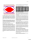
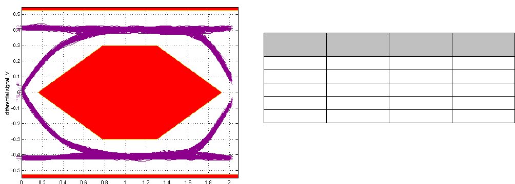
Figure 2. FX2 Eye Diagram of High-speed Signaling
In the diagram, notice how no signal traces overlap the cen-
tral, six-sided, shaded area. Also, no trace overlaps the
extremes of permissible voltage as shown in the shaded lines
at the very top and very bottom of the figure. Overlap of sig-
nal trace over the shaded areas would be a violation of the
USB 2.0 specification. Overlap can be caused by excessive
data jitter, mismatched impedance, and improper EMI filter-
ing.
The Cypress Semiconductor application note titled “High-
Speed USB PCB Layout Recommendations” treats the elec-
trical design concerns applicable to high-speed USB 2.0 cir-
cuits. There are numerous textbooks that treat the subject of
high-speed design in general. One such book is listed in the
References section of this document.
EZ-USB FX2 Device Supply Decoupling
Decoupling capacitors should be ceramic type of a stable
dielectric. For lower value capacitance, it is appropriate to
use Class 1 dielectric capacitors, C0G (also referred to as
NPO). Class 2 X7R should be used for the larger values. It is
recommended that 0.01-µF and 0.001-µF capacitors be used
to decouple supply pins nearest the pair of USB transceiver
circuits. The 0.001-µF should be C0G dielectric. This will help
decouple the power supply at the frequency range of high-
speed USB switching. The other power supply pins should be
decoupled with 0.1-µF X7R capacitors. It is important to have
short trace runs for the power and ground connections from
the EZ-USB FX2 component to solid power and ground
planes.
The specific recommendation for the ceramic capacitor near-
est each EZ-USB FX2 power pin is given in Table 1 below.
EMI and ESD Considerations
EMI and ESD need to be considered on a case by case basis
relative to the product enclosure, deployed environment, and
regulatory statutes. This application note does not give spe-
cific recommendations regarding EMI, but only gives general
EMI and ESD.
The CY7C68013 requires an external 24-MHz crystal. The
component includes circuitry to step up that frequency to sup-
port the 480-MHz bit rate of high-speed USB signaling. Solid
ground planes and short connections help keep emissions
low. Common mode chokes on the USB data pair reduce
emissions at the expense of signal quality. Other forms of
EMI filtering such as insertion of ferrite beads in-line with
USB data lines and addition of capacitance to the data lines
are strongly discouraged as these may cause a significant
corruption of signal quality.
An example of ESD consideration is in the coupling between
signal and safety/shield ground. The two grounds can be
coupled together with the parallel connection of a 4.7-nF,
250VAC capacitor and a 1M-ohm resistor. Review the
CY7C68013 data sheet regarding ESD susceptibility (the
maximum static discharge voltage) for the component pins.
When USB type B connectors are used, they should be USB
2.0 compliant. These shielded connectors are designed with
consideration for both EMI and ESD at the high-speed signal-
ling rates. In this connector the safety/shield ground is kept
separate from the signal ground.
PCB Design Recommendation
Printed circuit board (PCB) design for high-speed signaling
requires careful attention to component placement, signal
routing, layer stack-up, and selection of board material.
These characteristics impact electrical signal quality of the
USB data pair and the efficient dissipation of heat from the
EZ-USB FX2 component.
Some areas of special note concerning design with high-
speed devices are addressed in this section.
Table 1. Capacitor Recommendation
QFN
Pin Number
Capacitor
Value
QFN
Pin Number
Capacitor
Value
7 0.01 µF 43 0.1 µF
11 0.001 µF 55 0.1 µF
17 0.1 µF 3 0.1 µF
27 0.1 µF 3 2.2 µF
32 0.1 µF
[+] Feedback [+] Feedback


