


November 21, 2002 Document No. 001-43117 Rev. ** 4
AN1196
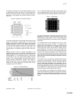
This figure shows the dielectric material thickness (“Prepreg”)
between layers 1 and 2 and the thickness between layers 3
and 4. The dimensions between these layers are a key ele-
ment in the design to set the proper characteristic impedance
for the USB data traces. This is the “h” term mentioned in the
prior section on PCB impedance design. The core material of
the PCB lies between layer 2 and 3. Although this material is
not critical to impedance characteristics, it is used to deter-
mine the overall board thickness.
Split Planes and Signal Routing
The shield/safety ground is on one of the four layers of the
PCB. However, when viewed across all layers of the PCB,
the section with the shield/safety ground plane should not
overlap any other planes or signals. If the shield/safety
ground is on the edge of the board with the USB connectors,
then there should not be any other metal in other PCB layers
directly above or below that area.
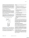
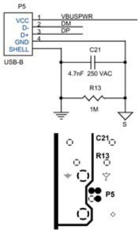
An alternate method of isolating the shield from the signal
ground is shown is Figure 4. The lower section of Figure 4
illustrates a portion of the ground layer. Given this scenario,
shield/safety ground plane is on the same layer as the signal
ground plane and is associated with the PCB’s layer two.
Figure 4. Section of Split Ground Plane
The upper portion of Figure 4 shows the schematic associ-
ated with the coupling across a split plane using C21 and
R13 components. The width of the gap between the
shield/safety ground and the signal ground should be no less
than 25 mil in order to minimize electrical edge coupling.
It is not necessary to have a large shield/safety ground plane.
A 100-mil-wide trace for interconnect is sufficient.
The following is a list of routing requirements which should be
adhered to:
■ USB connector pins 1, 2, 3, and 4 are in the area of the
signal ground, not the shield/safety ground.
■ The USB signals traces from the connector route over the
signal ground plane, never over the shield/safety ground.
■ No signal should route over the shield/safety ground
plane.
■ No other power or signal ground planes should overlap
the shield/safety ground plane.
■ All USB data signals should be routed exclusively on layer
one, the top side.
■ They should not route underneath any component except
for their associated USB connector.
■ Line length should be minimized.
■ To minimize coupling between the USB data pair and other
non-USB signals, the USB data pair should not be closer
than 35 mil to another signal.
■ If a ground fill is to be used on the top side of the board,
then to avoid significant impact to signal impedance, the
USB data pair should not be within 35 mil of the surface
ground plane.
These guidelines also apply to the crystal used for the
CY7C68013.
USB data lines must maintain proper differential pairing. This
is not possible at either end of the trace. At either end of the
trace, the physical limitation of routing to the pins of the USB
connector and the CY7C68013 causes a divergence from
this.This divergence should be minimized and the signal pairs
should adhere to the proper trace design for the required 90-
ohm differential impedance.
Thermal Design Considerations
The QFN (Quad Flatpack No leads) is a package with a small
footprint and low profile. It has excellent thermal properties: a
very low Θ
ja
of approximately 25°C per watt. These thermal
properties are ideal for the high-performance FX2.
The appropriate thermal design for use with the EZ-USB FX2
is to dissipate heat from the QFN package by conduction, not
convection. Heat is conducted away from the package
through its bond to the PCB. From there it is dissipated into
the signal ground plane. Special attention to the heat transfer
area below the package is required.
On the bottom of the package is a metal pad referred to as
the exposed die attach paddle, (or simply exposed paddle).
The exposed paddle is the means by which most of the EZ-
USB FX2 thermal energy is dissipated away from the pack-
age. The exposed paddle is a square metal area approxi-
mately 6 mm on a side.
[+] Feedback [+] Feedback