


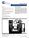
CY14B104L, CY14B104N
Document #: 001-07102 Rev. *L Page 6 of 25
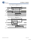
Preventing AutoStore
The AutoStore function is disabled by initiating an AutoStore
disable sequence. A sequence of read operations is performed
in a manner similar to the software STORE initiation. To initiate
the AutoStore disable sequence, the following sequence of CE
controlled read operations must be performed:
1. Read address 0x4E38 Valid READ
2. Read address 0xB1C7 Valid READ
3. Read address 0x83E0 Valid READ
4. Read address 0x7C1F Valid READ
5. Read address 0x703F Valid READ
6. Read address 0x8B45 AutoStore Disable
The AutoStore is re-enabled by initiating an AutoStore enable
sequence. A sequence of read operations is performed in a
manner similar to the software RECALL initiation. To initiate the
AutoStore enable sequence, the following sequence of CE
controlled read operations must be performed:
1. Read address 0x4E38 Valid READ
2. Read address 0xB1C7 Valid READ
3. Read address 0x83E0 Valid READ
4. Read address 0x7C1F Valid READ
5. Read address 0x703F Valid READ
6. Read address 0x4B46 AutoStore Enable
If the AutoStore function is disabled or re-enabled, a manual
STORE operation (hardware or software) must be issued to save
the AutoStore state through subsequent power down cycles. The
part comes from the factory with AutoStore enabled.
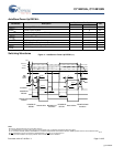
Data Protection
The CY14B104L/CY14B104N protects data from corruption
during low voltage conditions by inhibiting all externally initiated
STORE and write operations. The low voltage condition is
detected when V
CC
< V
SWITCH
. If the CY14B104L/CY14B104N
is in a write mode (both CE
and WE are LOW) at power up, after
a RECALL or STORE, the write is inhibited until the SRAM is
enabled after t
LZHSB
(HSB to output active). This protects against
inadvertent writes during power up or brown out conditions.
Noise Considerations
Refer to CY application note AN1064.
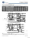
L H L 0x4E38
0xB1C7
0x83E0
0x7C1F
0x703F
0x4B46
Read SRAM
Read SRAM
Read SRAM
Read SRAM
Read SRAM
AutoStore Enable
Output Data
Output Data
Output Data
Output Data
Output Data
Output Data
Active
[8, 9]
L H L 0x4E38
0xB1C7
0x83E0
0x7C1F
0x703F
0x8FC0
Read SRAM
Read SRAM
Read SRAM
Read SRAM
Read SRAM
Nonvolatile Store
Output Data
Output Data
Output Data
Output Data
Output Data
Output High Z
Active I
CC2
[8, 9]
L H L 0x4E38
0xB1C7
0x83E0
0x7C1F
0x703F
0x4C63
Read SRAM
Read SRAM
Read SRAM
Read SRAM
Read SRAM
Nonvolatile
Recall
Output Data
Output Data
Output Data
Output Data
Output Data
Output High Z
Active
[8, 9]
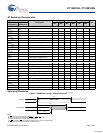
Table 1. Mode Selection (continued)
CE WE OE, BHE, BLE
[3]
A
15
- A
0
[7]
Mode IO Power
[+] Feedback