


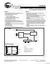
CY2048WAF
Document #: 38-07738 Rev. *A Page 2 of 7
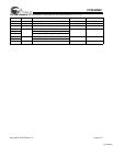
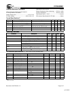
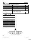
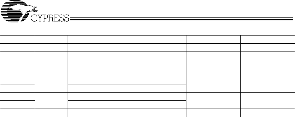
Die Pad Summary (Pad coordinates are referenced from the center of the die (X = 0, Y = 0))
Name Pad Number Description X coordinate (µm) Y coordinate (µm)
VDD 1 Voltage Supply –360.8 353.7
XOUT 2 Oscillator Drain –360.8 134.1
XIN 3 Oscillator Gate –360.8 –42.6
PD#/OE 4 Programmable power-down or output enable pin –360.8 –275.9
VPP High voltage for programming NV memory
SDATA Serial data pin used for programming in test mode
OUT 6 Clock output 360.0 353.7
SCL Serial clock for programming in test mode
VSS 5 Ground 360.0 –354.5
[+] Feedback