


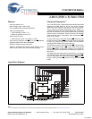
Document #: 001-08029 Rev. *E Page 4 of 13
CY62138FV30 MoBL
®
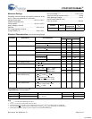
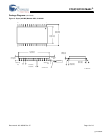
Thermal Resistance
[8]
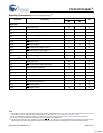
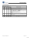
Parameter Description Test Conditions SOIC VFBGA TSOP II STSOP TSOP I Unit
Θ
JA
Thermal Resistance
(Junction to Ambient)
Still air, soldered on a 3 x 4.5
inch, two layer printed circuit
board
44.53 38.49 44.16 59.72 50.19 °C/W
Θ
JC
Thermal Resistance
(Junction to Case)
24.05 17.66 11.97 15.38 14.59 °C/W
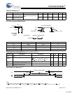
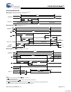
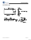
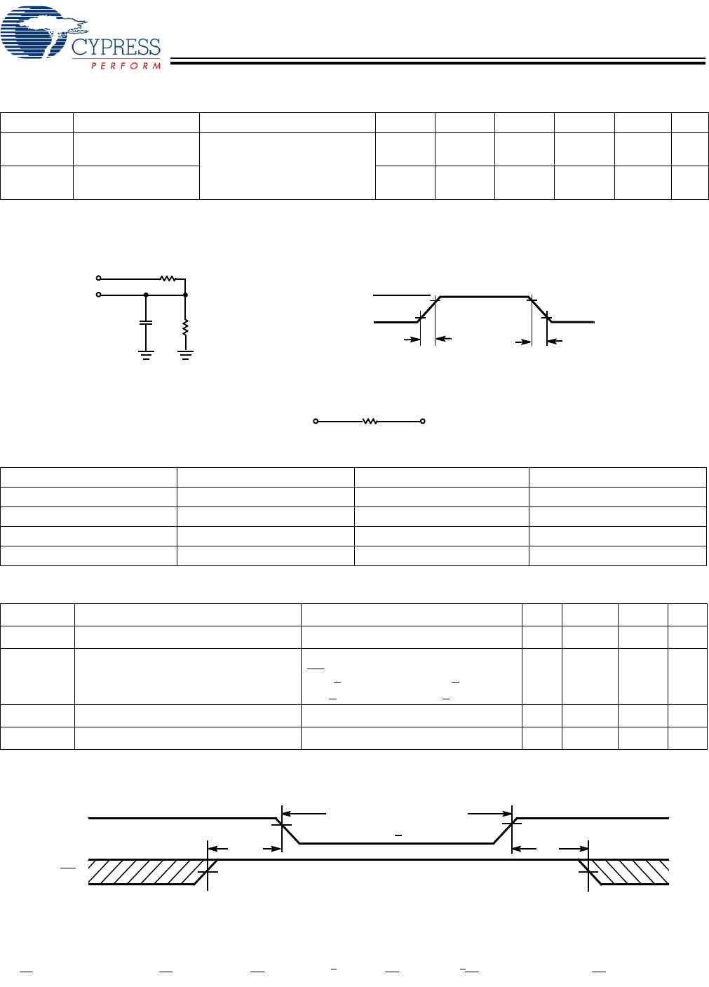
AC Test Loads and Waveforms
Parameters 2.5V (2.2V to 2.7V) 3.0V (2.7V to 3.6V) Unit
R1 16667 1103 Ω
R2 15385 1554 Ω
R
TH
8000 645 Ω
V
TH
1.20 1.75 V
Data Retention Characteristics (Over the Operating Range)
Parameter Description Conditions Min Typ
[3]
Max Unit
V
DR
V
CC
for Data Retention 1.5 V
I
CCDR
[7]
Data Retention Current V
CC
= 1.5V,
CE
1
> V
CC
− 0.2V or CE
2
< 0.2V,
V
IN
> V
CC
− 0.2V or V
IN
< 0.2V
14µA
t
CDR
[8]
Chip Deselect to Data Retention Time 0 ns
t
R
[9]
Operation Recovery Time t
RC
ns
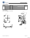
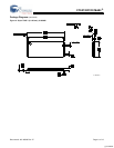
Data Retention Waveform
[10]
V
CC
V
CC
OUTPUT
R2
30 pF
INCLUDING
JIG AND
SCOPE
GND
90%
10%
90%
10%
Rise Time = 1 V/ns
Fall Time = 1 V/ns
OUTPUT V
Equivalent to:
THEVENIN EQUIVALENT
ALL INPUT PULSES
R
TH
R1
V
CC(min)
V
CC(min)
t
CDR
V
DR
> 1.5V
DATA RETENTION MODE
t
R
V
CC
CE
Notes:
9. Full device AC operation requires linear V
CC
ramp from V
DR
to V
CC(min)
> 100 µs or stable at V
CC(min)
> 100 µs.
10.CE
is the logical combination of CE
1
and CE
2
. When CE
1
is LOW and CE
2
is HIGH, CE is LOW; when CE
1
is HIGH or CE
2
is LOW, CE is HIGH.
[+] Feedback