


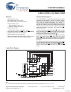
Document #: 001-08029 Rev. *E Page 5 of 13
CY62138FV30 MoBL
®
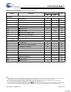
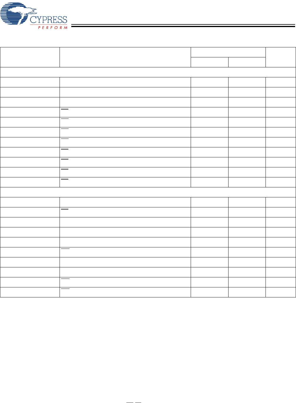
Switching Characteristics (Over the Operating Range)
[11]
Parameter Description
45 ns
Unit
Min Max
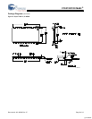
Read Cycle
t
RC
Read Cycle Time 45 ns
t
AA
Address to Data Valid 45 ns
t
OHA
Data Hold from Address Change 10 ns
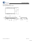
t
ACE
CE
1
LOW and CE
2
HIGH to Data Valid
45 ns
t
DOE
OE LOW to Data Valid 22 ns
t
LZOE
OE LOW to Low-Z
[12]
5ns
t
HZOE
OE HIGH to High-Z
[12,13]
18 ns
t
LZCE
CE
1
LOW and CE
2
HIGH to Low Z
[12]
10 ns
t
HZCE
CE
1
HIGH or CE
2
LOW to High-Z
[12, 13]
18 ns
t
PU
CE
1
LOW and CE
2
HIGH to Power Up
0ns
t
PD
CE
1
HIGH or CE
2
LOW to Power Down
45 ns
Write Cycle
[14]
t
WC
Write Cycle Time 45 ns
t
SCE
CE
1
LOW and CE
2
HIGH to Write End
35 ns
t
AW
Address Setup to Write End 35 ns
t
HA
Address Hold from Write End 0 ns
t
SA
Address Setup to Write Start 0 ns
t
PWE
WE Pulse Width 35 ns
t
SD
Data Setup to Write End 25 ns
t
HD
Data Hold from Write End 0 ns
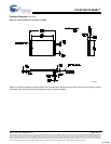
t
HZWE
WE LOW to High-Z
[12, 13]
18 ns
t
LZWE
WE HIGH to Low-Z
[12]
10 ns
Notes
11. Test conditions for all parameters other than tri-state parameters assume signal transition time of 3 ns or less (1 V/ns), timing reference levels of V
CC(typ)
/2, input
pulse levels of 0 to V
CC(typ)
, and output loading of the specified I
OL
/I
OH
as shown in the ““AC Test Loads and Waveforms” on page 4” .
12.At any given temperature and voltage condition, t
HZCE
is less than t
LZCE
, t
HZOE
is less than t
LZOE
, and t
HZWE
is less than t
LZWE
for any given device.
13.t
HZOE
, t
HZCE
, and t
HZWE
transitions are measured when the output enters a high impedance state.
14.The internal write time of the memory is defined by the overlap of WE
, CE
1
= V
IL
, and CE
2
= V
IH
. All signals must be ACTIVE to initiate a write and any of these
signals can terminate a write by going INACTIVE. Reference the data input setup and hold timing to the edge of the signal that terminates the write.
[+] Feedback