


CY62167DV18 MoBL
®
Document #: 38-05326 Rev. *C Page 3 of 11
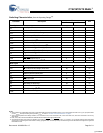
Maximum Ratings
Exceeding the maximum ratings may impair the useful life of
the device. These user guidelines are not tested.
Storage Temperature .................................–65°C to +150°C
Ambient Temperature with
Power Applied.............................................–55°C to +125°C
Supply Voltage to Ground Potential. –0.2V to V
CCmax
+ 0.2V
DC Voltage Applied to Outputs
in High-Z State
[4, 5]
........................... –0.2V to V
CCmax
+ 0.2V
DC Input Voltage
[4, 5]
........................–0.2V to V
CCmax
+ 0.2V
Output Current into Outputs (LOW).............................20 mA
Static Discharge Voltage.......................................... > 2001V
(MIL-STD-883, Method 3015)
Latch up Current.....................................................> 200 mA
Operating Range
Range
Ambient
Temperature
V
CC
[6]
Industrial –40°C to +85°C 1.65V to 1.95V
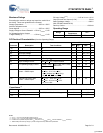
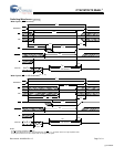
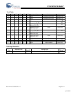
DC Electrical Characteristics (Over the Operating Range)
Parameter Description Test Conditions
55 ns
UnitMin Typ
[2]
Max
V
OH
Output HIGH Voltage I
OH
= −0.1 mA 1.4 V
V
OL
Output LOW Voltage I
OL
= 0.1 mA 0.2 V
V
IH
Input HIGH Voltage 1.4 V
CC
+ 0.2 V
V
IL
Input LOW Voltage –0.2 0.4 V
I
IX
Input Leakage Current GND < V
I
< V
CC
–1 +1 µA
I
OZ
Output Leakage Current GND < V
O
< V
CC
, Output Disabled –1 +1 µA
I
CC
V
CC
Operating Supply Current f = f
MAX
= 1/t
RC
V
CC
= 1.95V, I
OUT
= 0 mA,
CMOS level
15 30 mA
f = 1 MHz 1.5 5
I
SB1
Automatic CE Power down
Current − CMOS Inputs
CE
1
> V
CC
− 0.2V, CE
2
< 0.2V,
V
IN
> V
CC
− 0.2V, V
IN
< 0.2V,
f = f
MAX
(Address and Data Only),
f = 0 (OE
, WE, BHE and BLE)
2.5 20 µA
I
SB2
Automatic CE Power down
Current − CMOS Inputs
CE
1
> V
CC
− 0.2V, CE
2
< 0.2V,
V
IN
> V
CC
− 0.2V or V
IN
< 0.2V,
f = 0, V
CC
=1.95V
2.5 20 µA
Notes
4. V
IL(min)
= –2.0V for pulse durations less than 20 ns.
5. V
IH(max)
= V
CC
+ 0.75V for pulse durations less than 20 ns.
6. Full device AC operation requires linear V
CC
ramp from 0 to V
CC(min)
and V
CC
must be stable at V
CC(min)
for 500 µs.
7. Tested initially and after any design or process changes that may affect these parameters.
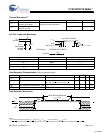
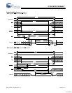
Capacitance
[7]
Parameter Description Test Conditions Max Unit
C
IN
Input Capacitance T
A
= 25°C, f = 1 MHz, V
CC
= V
CC(typ)
6pF
C
OUT
Output Capacitance 8 pF
[+] Feedback