


CY7C024AV/024BV/025AV/026AV
CY7C0241AV/0251AV/036AV
Document #: 38-06052 Rev. *J Page 10 of 19
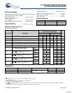
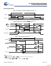
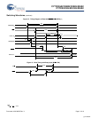
Data Retention Mode
The CY7C024AV/024BV/025AV/026AV and
CY7C0241AV/0251AV/036AV are designed for battery backup.
Data retention voltage and supply current are guaranteed over
temperature. The following rules ensure data retention:
1. Chip Enable (CE) must be held HIGH during data retention,
within V
CC
to V
CC
– 0.2V.
2. CE
must be kept between V
CC
– 0.2V and 70 percent of V
CC
during the power up and power down transitions.
3. The RAM can begin operation >t
RC
after V
CC
reaches the
minimum operating voltage (3.0V).
Notes
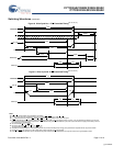
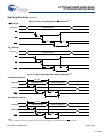
25.For information on port to port delay through RAM cells from writing port to reading port, refer to Figure 12.
26.Test conditions used are Load 2.
27.t
BDD
is a calculated parameter and is the greater of t
WDD
– t
PWE
(actual) or t
DDD
– t
SD
(actual).
28.CE
= V
CC
, V
in
= GND to V
CC
, T
A
= 25°C. This parameter is guaranteed but not tested.
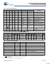
t
PWE
Write Pulse Width 15 20 ns
t
SD
Data Setup to Write End 15 15 ns
t
HD
Data Hold From Write End 0 0 ns
t
HZWE
[23, 24]
R/W LOW to High Z 12 15 ns
t
LZWE
[23, 24]
R/W HIGH to Low Z 3 0 ns
t
WDD
[25]
Write Pulse to Data Delay 45 50 ns
t
DDD
[25]
Write Data Valid to Read Data Valid 30 35 ns
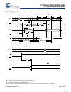
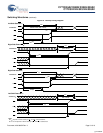
Busy Timing
[26]
t
BLA
BUSY LOW from Address Match 20 20 ns
t
BHA
BUSY HIGH from Address Mismatch 20 20 ns
t
BLC
BUSY LOW from CE LOW 20 20 ns
t
BHC
BUSY HIGH from CE HIGH 17 17 ns
t
PS
Port Setup for Priority 5 5 ns
t
WB
R/W HIGH after BUSY (Slave) 0 0 ns
t
WH
R/W HIGH after BUSY HIGH (Slave) 15 17 ns
t
BDD
[27]
BUSY HIGH to Data Valid 20 25 ns
Interrupt Timing
[26]
t
INS
INT Set Time 20 20 ns
t
INR
INT Reset Time 20 20 ns
Semaphore Timing
t
SOP
SEM Flag Update Pulse (OE or SEM)1012ns
t
SWRD
SEM Flag Write to Read Time 5 5 ns
t
SPS
SEM Flag Contention Window 5 5 ns
t
SAA
SEM Address Access Time 20 25 ns
Switching Characteristics
Over the Operating Range (continued)
[20]
Parameter Description
CY7C024AV/024BV/025AV/026AV
CY7C0241AV/0251AV/036AV
Unit
-20 -25
Min Max Min Max
Timing
Parameter Test Conditions
[28]
Max Unit
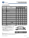
ICC
DR1
at VCC
DR
= 2V 50 μA
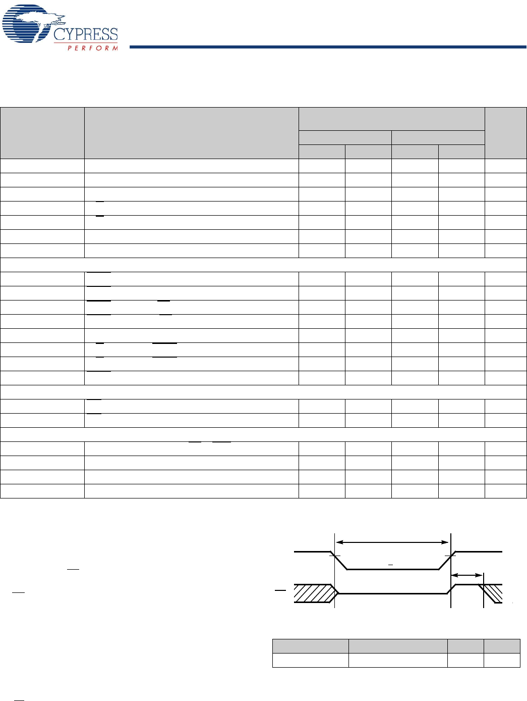
Data Retention Mode
3.0V
3.0V
V
CC
> 2.0V
V
CC
to V
CC
– 0.2V
V
CC
CE
t
RC
V
IH
[+] Feedback