


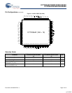
CY7C024AV/024BV/025AV/026AV
CY7C0241AV/0251AV/036AV
Document #: 38-06052 Rev. *J Page 12 of 19
Notes
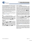
34.R/W
or CE must be HIGH during all address transitions.
35.A write occurs during the overlap (t
SCE
or t
PWE
) of a LOW CE or SEM and a LOW UB or LB.
36.t
HA
is measured from the earlier of CE or R/W or (SEM or R/W) going HIGH at the end of write cycle.
37.If OE
is LOW during a R/W controlled write cycle, the write pulse width must be the larger of t
PWE
or (t
HZWE
+ t
SD
) to enable the IO drivers to turn off and
data to be placed on the bus for the required t
SD
. If OE is HIGH during an R/W controlled write cycle, this requirement does not apply and the write pulse can
be as short as the specified t
PWE
.
38.To access RAM, CE
= V
IL
, SEM = V
IH
.
39.To access upper byte, CE
= V
IL
, UB = V
IL
, SEM = V
IH
.
To access lower byte, CE
= V
IL
, LB = V
IL
, SEM = V
IH
.
40.Transition is measured ±500 mV from steady state with a 5 pF load (including scope and jig). This parameter is sampled and not 100 percent tested.
41.During this period, the IO pins are in the output state, and input signals must not be applied.
42.If the CE
or SEM LOW transition occurs simultaneously with or after the R/W LOW transition, the outputs remain in the high impedance state.
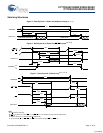
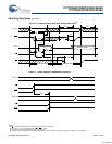
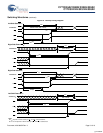
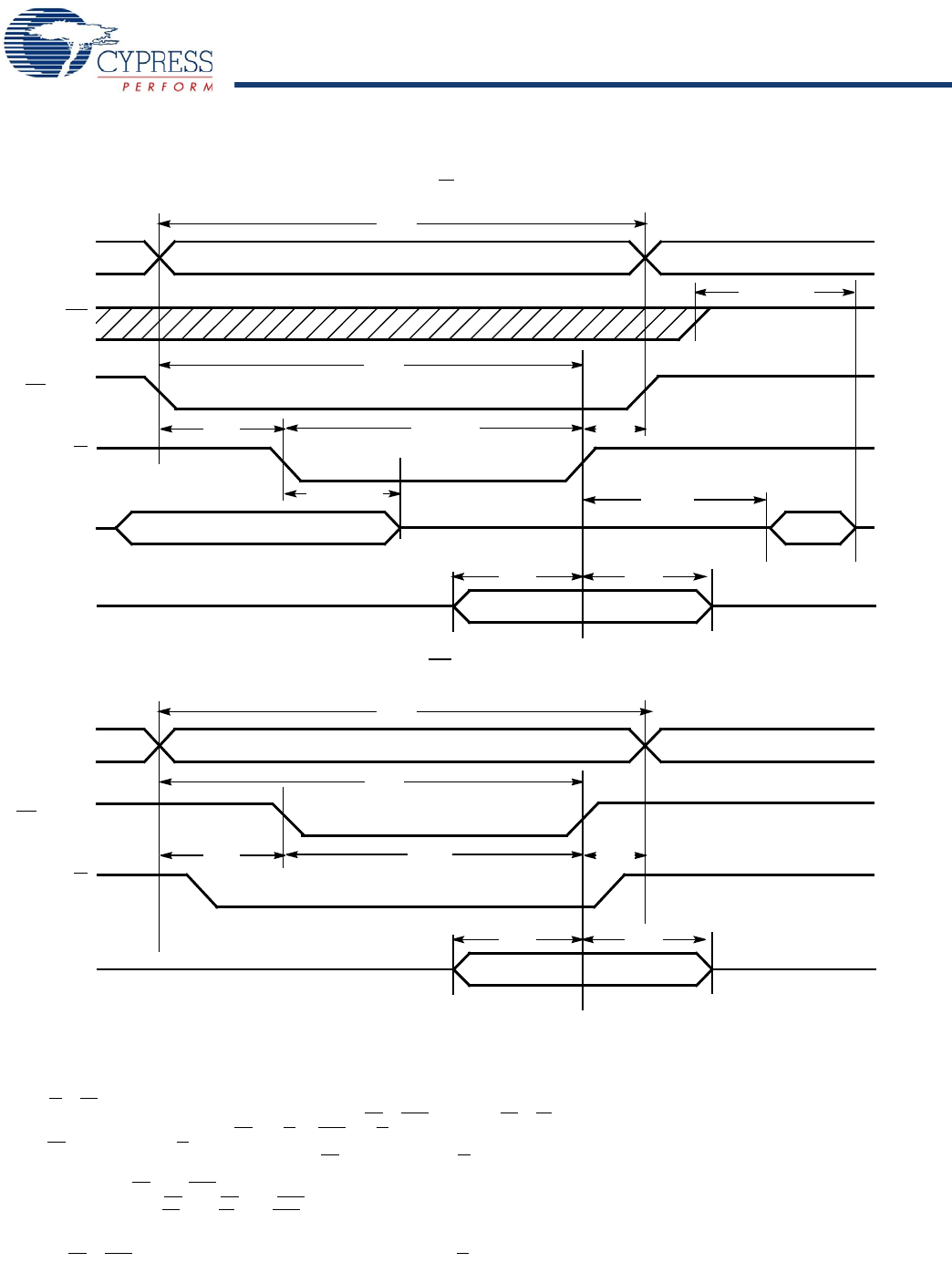
Switching Waveforms
(continued)
t
AW
t
WC
t
PWE
t
HD
t
SD
t
HA
CE
R/W
OE
DATAOUT
DATA IN
ADDRESS
t
HZOE
t
SA
t
HZWE
t
LZWE
Figure 8. Write Cycle No. 1: R/W Controlled Timing
[34, 35, 36, 37]
[40]
[40]
[37]
[38, 39]
NOTE 41
NOTE 41
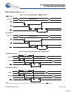
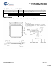
t
AW
t
WC
t
SCE
t
HD
t
SD
t
HA
CE
R/W
DATA IN
ADDRESS
t
SA
Figure 9. Write Cycle No. 2: CE Controlled Timing
[34, 35, 36, 42]
[38, 39]
[+] Feedback