


CY7C024AV/024BV/025AV/026AV
CY7C0241AV/0251AV/036AV
Document #: 38-06052 Rev. *J Page 14 of 19
Note
47.CE
L
= CE
R
= LOW.
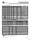
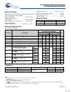
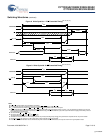
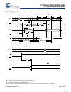
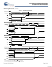
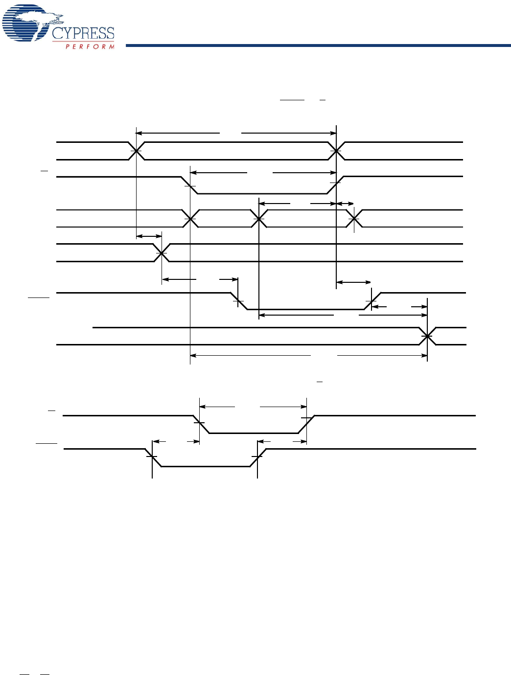
Switching Waveforms
(continued)
VALID
t
DDD
t
WDD
MATCH
MATCH
R/W
R
DATA IN
R
DATA
OUTL
t
WC
ADDRESS
R
t
PWE
VALID
t
SD
t
HD
ADDRESS
L
t
PS
t
BLA
t
BHA
t
BDD
BUSY
L
Figure 12. Timing Diagram of Read with BUSY (M/S=HIGH)
[47]
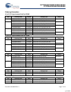
t
PWE
R/W
BUSY
t
WB
t
WH
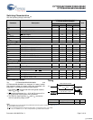
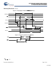
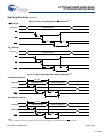
Figure 13. Write Timing with Busy Input (M/S=LOW)
[+] Feedback