


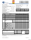
CY7C0837AV, CY7C0830AV
CY7C0831AV, CY7C0832AV
CY7C0832BV, CY7C0833AV
Document #: 38-06059 Rev. *S Page 16 of 28
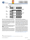
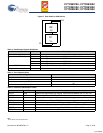
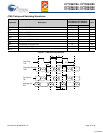
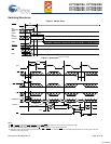
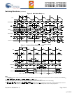
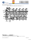
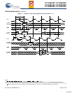
Switching Waveforms
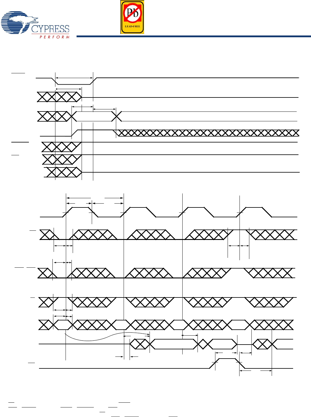
Figure 8. Master Reset
Figure 9. Read Cycle
[12, 30, 31, 32, 33]
MRST
t
RSR
t
RS
INACTIVE
ACTIVE
TMS
TDO
INT
CNTINT
t
RSF
t
RSS
ALL
ADDRESS/
DATA
LINES
ALL
OTHER
INPUTS
t
CH2
t
CL2
t
CYC2
t
SC
t
HC
t
SW
t
HW
t
SA
t
HA
A
n
A
n+1
CLK
CE
R/W
ADDRESS
DATA
OUT
OE
A
n+2
A
n+3
t
SC
t
HC
t
OHZ
t
OE
t
OLZ
t
DC
t
CD2
t
CKLZ
Q
n
Q
n+1
Q
n+2
1 Latency
BE0
–BE1
t
SB
t
HB
Notes
30.OE
is asynchronously controlled; all other inputs (excluding MRST and JTAG) are synchronous to the rising clock edge.
31.ADS
= CNTEN = LOW, and MRST = CNTRST = CNT/MSK = HIGH.
32.The output is disabled (high-impedance state) by CE
= V
IH
following the next rising edge of the clock.
33.Addresses need not be accessed sequentially because ADS
= CNTEN = V
IL
with CNT/MSK = V
IH
constantly loads the address on the rising edge of the CLK.
Numbers are for reference only.
[+] Feedback