CY7C1062DV33
Document Number: 38-05477 Rev.*E Page 11 of 12
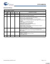
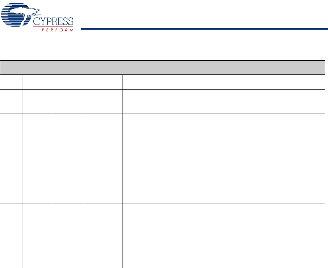
Document History
Document Title: CY7C1062DV33 16 Mbit (512K X 32) Static RAM
Document Number: 38-05477
Rev. ECN No.
Orig. of
Change
Submission
Date
Description of Change
** 201560 SWI See ECN Advance data sheet for C9 IPP
*A 233748 RKF See ECN 1.AC, DC parameters are modified as per EROS (Spec # 01-2165)
2.Pb-free offering in the Ordering Information
*B 469420 NXR See ECN Converted from Advance Information to Preliminary
Removed –8 and –12 speed bins from product offering
Removed Commercial operating Range
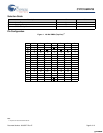
Changed J7 Ball of PBGA from DNU to NC in the pinout diagram
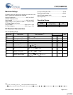
Included the Maximum ratings for Static Discharge Voltage and Latch Up Current
on page 2
Changed I
CC(Max)
from 220 mA to 150 mA
Changed I
SB1(Max)
from 70 mA to 30 mA
Changed I
SB2(Max)
from 40 mA to 25 mA
Specified the Overshoot specification in footnote 1
Changed t
SD
from 5.5 ns to 5 ns
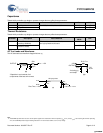
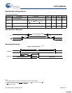
Added Data Retention Characteristics table and waveform on page 5.
Updated the 48-pin FBGA package
Updated the Ordering Information Table
*C 499604 NXR See ECN Added note 1 for NC pins
Updated Test Condition for I
CC
in DC Electrical Characteristics table
Added note for t
ACE
, t
LZCE
, t
HZCE
, t
PU
, t
PD
, and t
SCE
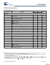
in AC Switching Characteristics
Table on page 4
*D 1462583 VKN/AESA See ECN Converted from preliminary to final
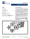
Updated block diagram
Changed I
CC
spec from 150 mA to 175 mA
Updated thermal specs
*E 2541850 VKN/PYRS 07/22/08 Added -10BGI part in the Ordering Information table
[+] Feedback [+] Feedback


