CY7C1161V18, CY7C1176V18
CY7C1163V18, CY7C1165V18
Document Number: 001-06582 Rev. *D Page 8 of 29
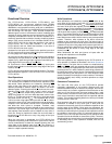
Functional Overview
The CY7C1161V18, CY7C1176V18, CY7C1163V18, and
CY7C1165V18 are synchronous pipelined burst SRAMs
equipped with both a read port and a write port. The read port is
dedicated to read operations and the write port is dedicated to
write operations. Data flows into the SRAM through the write port
and out through the read port. These devices multiplex the
address inputs in order to minimize the number of address pins
required. By having separate read and write ports, the QDR-II+
completely eliminates the need to “turn-around” the data bus. It
avoids any possible data contention, thereby, simplifying system
design. Each access consists of four 8-bit data transfers in the
case of CY7C1161V18, four 9-bit data transfers in the case of
CY7C1176V18, four 18-bit data transfers in the case of
CY7C1163V18, and four 36-bit data transfers in the case of
CY7C1165V18 in two clock cycles.
Accesses for both ports are initiated on the positive input clock
(K). All synchronous input and output timings are referenced to
the rising edge of the Input clocks (K/K
).
All synchronous data inputs (D
[x:0]
) pass through input registers
controlled by the input clocks (K and K
). All synchronous data
outputs (Q
[x:0]
) pass through output registers controlled by the
rising edge of the Input clocks (K and K
) also.
All synchronous control (RPS, WPS, BWS
[x:0]
) inputs pass
through input registers controlled by the rising edge of the input
clocks (K and K).
CY7C1163V18 is described in the following sections. The same
basic descriptions apply to CY7C1161V18, CY7C1176V18, and
CY7C1165V18.
Read Operations
The CY7C1163V18 is organized internally as four arrays of 256K
x 18. Accesses are completed in a burst of four sequential 18-bit
data words. Read operations are initiated by asserting RPS
active at the rising edge of the positive input clock (K). The
address presented to address inputs are stored in the Read
address register. Following the next two K clock rises, the corre-
sponding lowest order 18-bit word of data is driven onto the
Q
[17:0]
using K as the output timing reference. On the subse-
quent rising edge of K, the next 18-bit data word is driven onto
the Q
[17:0]
. This process continues until all four 18-bit data words
have been driven out onto Q
[17:0]
. The requested data is valid
0.45 ns from the rising edge of the Input clock K or K
. In order to
maintain the internal logic, each read access must be allowed to
complete. Each read access consists of four 18-bit data words
and takes two clock cycles to complete. Therefore, read
accesses to the device cannot be initiated on two consecutive K
clock rises. The internal logic of the device ignores the second
read request. Read accesses can be initiated on every other K
clock rise. Doing so pipelines the data flow such that data is
transferred out of the device on every rising edge of the input
clocks K and K
.
When the read port is deselected, the CY7C1163V18 first
completes the pending read transactions. Synchronous internal
circuitry automatically tri-states the outputs following the next
rising edge of the negative input clock (K
). This allows for a
seamless transition between devices without the insertion of wait
states in a depth expanded memory.
Write Operations
Write operations are initiated by asserting WPS active at the
rising edge of the positive input clock (K). On the following K
clock rise, the data presented to D
[17:0]
is latched and stored into
the lower 18-bit write data register, provided BWS
[1:0]
are both
asserted active. On the subsequent rising edge of the negative
input clock (K), the information presented to D
[17:0]
is also stored
into the write data register, provided BWS
[1:0]
are both asserted
active. This process continues for one more cycle until four 18-bit
words (a total of 72 bits) of data are stored in the SRAM. The 72
bits of data are then written into the memory array at the specified
location. Therefore, write accesses to the device cannot be
initiated on two consecutive K clock rises. The internal logic of
the device ignores the second write request. Write accesses are
initiated on every other rising edge of the positive input clock (K).
Doing so pipelines the data flow such that 18 bits of data can be
transferred into the device on every rising edge of the input
clocks (K and K
).
When deselected, the write port ignores all inputs after the
pending write operations are completed.
Byte Write Operations
Byte write operations are supported by the CY7C1163V18. A
write operation is initiated as described in the Write Operations
section above. The bytes that are written are determined by
BWS
0
and BWS
1
, which are sampled with each set of 18-bit data
words. Asserting the appropriate byte write select input during
the data portion of a write enables the data being presented to
be latched and written into the device. Deasserting the byte write
select input during the data portion of a write allows the data
stored in the device for that byte to remain unaltered. This feature
is used to simplify read, modify, and write operations to a byte
write operation.
Concurrent Transactions
The read and write ports on the CY7C1163V18 operate
completely independent of one another. Because each port
latches the address inputs on different clock edges, the user can
read or write to any location, regardless of the transaction on the
other port. If the ports access the same location when a read
follows a write in successive clock cycles, the SRAM delivers the
most recent information associated with the specified address
location. This includes forwarding data from a write cycle initiated
on the previous K clock rise.
Read accesses and write access are scheduled such that one
transaction is initiated on any clock cycle. If both ports are
selected on the same K clock rise, the arbitration depends on the
previous state of the SRAM. If both ports are deselected, the
read port takes priority. If a read is initiated on the previous cycle,
the write port assumes priority (because read operations cannot
be initiated on consecutive cycles). If a write was initiated on the
previous cycle, the read port assumes priority (because write
operations cannot be initiated on consecutive cycles). Therefore,
asserting both port selects active from a deselected state results
in alternating read or write operations initiated, with the first
access being a read.
[+] Feedback [+] Feedback


