


CY7C1246V18, CY7C1257V18
CY7C1248V18, CY7C1250V18
Document Number: 001-06348 Rev. *D Page 22 of 27
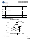
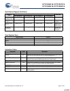
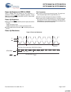
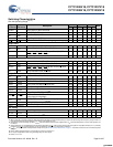
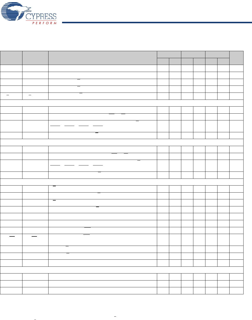
Switching Characteristics
Over the Operating Range
[20, 21]
Cypress
Parameter
Consortium
Parameter
Description
375 MHz 333 MHz 300 MHz
Unit
Min Max Min Max Min Max
t
POWER
V
DD
(Typical) to the first Access
[22]
1–1–1–ms
t
CYC
t
KHKH
K Clock Cycle Time 2.66 8.4 3.0 8.4 3.3 8.4 ns
t
KH
t
KHKL
Input Clock (K/K) HIGH 0.4 – 0.4 – 0.4 – t
CYC
t
KL
t
KLKH
Input Clock (K/K) LOW 0.4–0.4–0.4–t
CYC
t
KHKH
t
KHKH
K Clock Rise to K Clock Rise (rising edge to rising edge) 1.13 – 1.28 – 1.40 – ns
Setup Times
t
SA
t
AVKH
Address Setup to K Clock Rise 0.4 – 0.4 – 0.4 – ns
t
SC
t
IVKH
Control Setup to K Clock Rise (LD, R/W) 0.4–0.4–0.4– ns
t
SCDDR
t
IVKH
Double Data Rate Control Setup to Clock (K, K) Rise
(BWS
0
, BWS
1
, BWS
2
, BWS
3
)
0.28 – 0.28 – 0.28 – ns
t
SD
t
DVKH
D
[X:0]
Setup to Clock (K/K) Rise 0.28–0.28–0.28– ns
Hold Times
t
HA
t
KHAX
Address Hold after K Clock Rise
0.4–0.4–0.4– ns
t
HC
t
KHIX
Control Hold after K Clock Rise (LD, R/W) 0.4–0.4–0.4– ns
t
HCDDR
t
KHIX
Double Data Rate Control Hold after Clock (K/K) Rise
(BWS
0
, BWS
1
, BWS
2
, BWS
3
)
0.28 – 0.28 – 0.28 – ns
t
HD
t
KHDX
D
[X:0]
Hold after Clock (K/K) Rise 0.28–0.28–0.28– ns
Output Times
t
CO
t
CHQV
K/K Clock Rise to Data Valid – 0.45 – 0.45 – 0.45 ns
t
DOH
t
CHQX
Data Output Hold after K/K Clock Rise (Active to Active) –0.45 – –0.45 – –0.45 – ns
t
CCQO
t
CHCQV
K/K Clock Rise to Echo Clock Valid
–0.45–0.45–0.45ns
t
CQOH
t
CHCQX
Echo Clock Hold after K/K Clock Rise –0.45 – –0.45 – –0.45 – ns
t
CQD
t
CQHQV
Echo Clock High to Data Valid – 0.2 – 0.2 – 0.2 ns
t
CQDOH
t
CQHQX
Echo Clock High to Data Invalid –0.2 – –0.2 – –0.2 – ns
t
CQH
t
CQHCQL
Output Clock (CQ/CQ) HIGH
[23]
0.88 – 1.03 – 1.15 – ns
t
CQHCQH
t
CQHCQH
CQ Clock Rise to CQ Clock Rise
[23]
(rising edge to rising edge)
0.88 – 1.03 – 1.15 – ns
t
CHZ
t
CHQZ
Clock (K/K) Rise to High-Z (Active to High-Z)
[24, 25]
–0.45–0.45–0.45ns
t
CLZ
t
CHQX1
Clock (K/K) Rise to Low-Z
[24, 25]
–0.45 – –0.45 – –0.45 – ns
t
QVLD
t
CQHQVLD
Echo Clock High to QVLD Valid
[26]
–0.20 0.20 –0.20 0.20 –0.20 0.20 ns
DLL Timing
t
KC Var
t
KC Var
Clock Phase Jitter – 0.20 – 0.20 – 0.20 ns
t
KC lock
t
KC lock
DLL Lock Time (K) 2048 – 2048 – 2048 – Cycles
t
KC Reset
t
KC Reset
K Static to DLL Reset
[27]
30–30–30– ns
Notes
21.When a part with a maximum frequency above 300 MHz is operating at a lower clock frequency, it requires the input timing of the frequency range in which it is
being operated and outputs data with the output timing of that frequency range.
22.This part has an internal voltage regulator; t
POWER
is the time that the power must be supplied above V
DD
minimum initially before a read or write operation can
be initiated.
23.These parameters are extrapolated from the input timing parameters (t
KHKH
- 250 ps, where 250 ps is the internal jitter. An input jitter of 200 ps (t
KC Var
) is already
included in the t
KHKH
). These parameters are only guaranteed by design and are not tested in production.
24.t
CHZ
, t
CLZ
, are specified with a load capacitance of 5 pF as in (b) of “AC Test Loads and Waveforms” on page 21. Transition is measured ±100 mV from steady-state
voltage.
25.At any voltage and temperature t
CHZ
is less than t
CLZ
and t
CHZ
less than t
CO
.
26.t
QVLD
spec is applicable for both rising and falling edges of QVLD signal.
27.Hold to >V
IH
or <V
IL
.
[+] Feedback [+] Feedback