CY7C1345G
Document Number: 38-05517 Rev. *E Page 13 of 20
Timing Diagrams
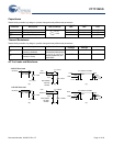
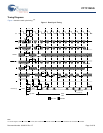
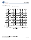
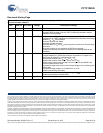
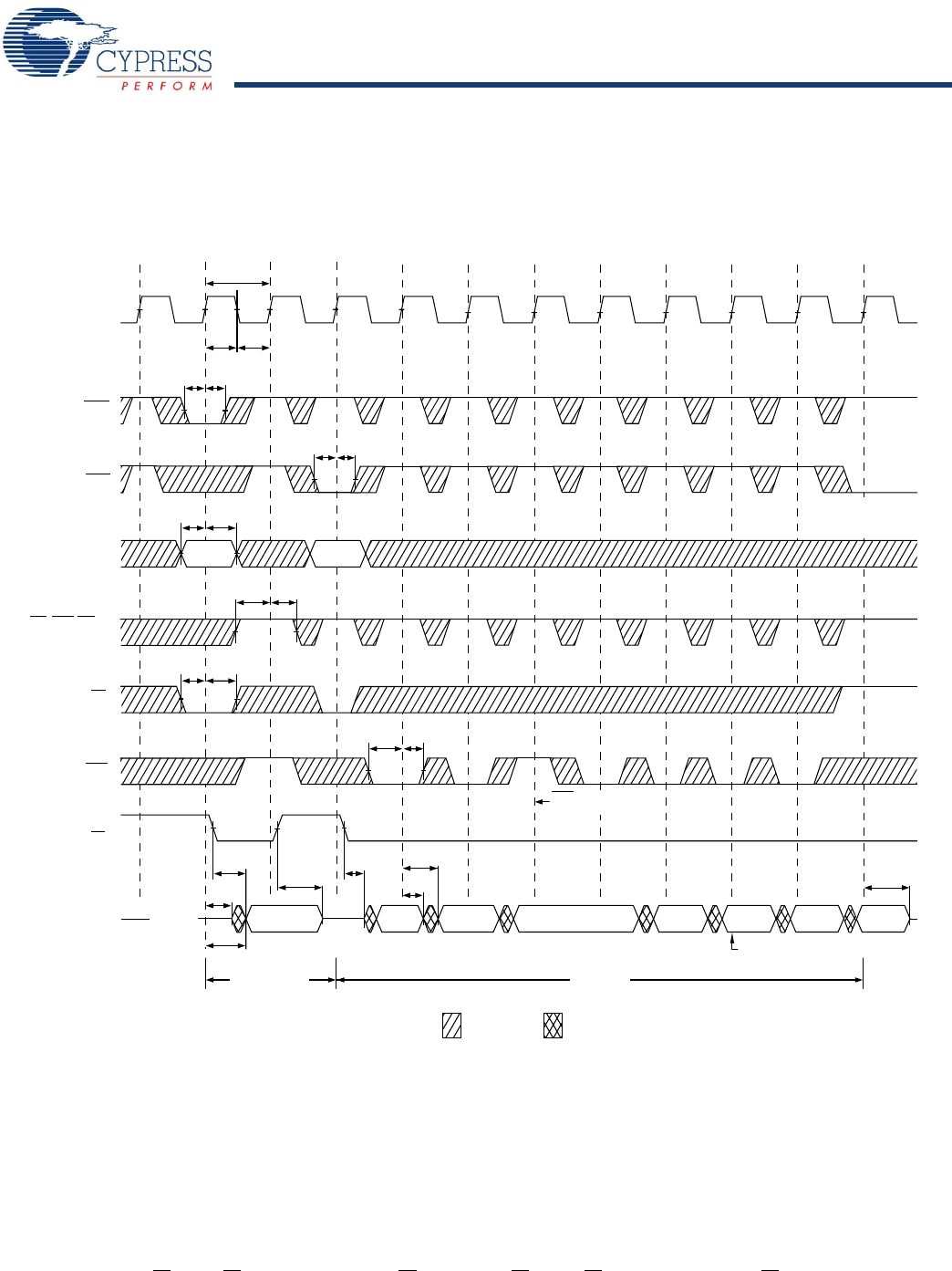
Figure 1 shows the read cycle timing.
[15]
Figure 1. Read Cycle Timing
t
CYC
t
CL
CLK
t
ADH
t
ADS
ADDRESS
t
CH
t
AH
t
AS
A1
t
CEH
t
CES
Data Out (Q)
High-Z
t
CLZ
t
DOH
t
CDV
t
OEHZ
t
CDV
Single READ
BURST
READ
t
OEV
t
OELZ
t
CHZ
Burst wraps around
to its initial state
t
ADVH
t
ADVS
t
WEH
t
WES
t
ADH
t
ADS
Q(A2)
Q(A2 + 1)
Q(A2 + 2)
Q(A1)
Q(A2)
Q(A2 + 1)
Q(A2 + 2)
Q(A2 + 3)
A2
ADV suspends burst
Deselect Cycle
DON’T CARE
UNDEFINED
ADSP
ADSC
GW, BWE,BW
[A:B]
CE
ADV
OE
Note:
15.On this diagram, when CE
is LOW: CE
1
is LOW, CE
2
is HIGH and CE
3
is LOW. When CE is HIGH: CE
1
is HIGH or CE
2
is LOW or CE
3
is HIGH.


