Document Number: 38-05517 Rev. *E Revised July 15, 2007 Page 20 of 20
Intel and Pentium are registered trademarks and i486 is a trademark of Intel Corporation. All product and company names mentioned in this document may be the trademarks of their respective holders.
CY7C1345G
© Cypress Semiconductor Corporation, 2004-2007. The information contained herein is subject to change without notice. Cypress Semiconductor Corporation assumes no responsibility for the use
of any circuitry other than circuitry embodied in a Cypress product. Nor does it convey or imply any license under patent or other rights. Cypress products are not warranted nor intended to be used
for medical, life support, life saving, critical control or safety applications, unless pursuant to an express written agreement with Cypress. Furthermore, Cypress does not authorize its products for use
as critical components in life-support systems where a malfunction or failure may reasonably be expected to result in significant injury to the user. The inclusion of Cypress products in life-support
systems application implies that the manufacturer assumes all risk of such use and in doing so indemnifies Cypress against all charges.
Any Source Code (software and/or firmware) is owned by Cypress Semiconductor Corporation (Cypress) and is protected by and subject to worldwide patent protection (United States and foreign),
United States copyright laws and international treaty provisions. Cypress hereby grants to licensee a personal, non-exclusive, non-transferable license to copy, use, modify, create derivative works of,
and compile the Cypress Source Code and derivative works for the sole purpose of creating custom software and or firmware in support of licensee product to be used only in conjunction with a Cypress
integrated circuit as specified in the applicable agreement. Any reproduction, modification, translation, compilation, or representation of this Source Code except as specified above is prohibited without
the express written permission of Cypress.
Disclaimer: CYPRESS MAKES NO WARRANTY OF ANY KIND, EXPRESS OR IMPLIED, WITH REGARD TO THIS MATERIAL, INCLUDING, BUT NOT LIMITED TO, THE IMPLIED WARRANTIES
OF MERCHANTABILITY AND FITNESS FOR A PARTICULAR PURPOSE. Cypress reserves the right to make changes without further notice to the materials described herein. Cypress does not
assume any liability arising out of the application or use of any product or circuit described herein. Cypress does not authorize its products for use as critical components in life-support systems where
a malfunction or failure may reasonably be expected to result in significant injury to the user. The inclusion of Cypress’ product in a life-support systems application implies that the manufacturer
assumes all risk of such use and in doing so indemnifies Cypress against all charges.
Use may be limited by and subject to the applicable Cypress software license agreement.
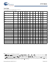
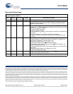
Document History Page
Document Title: CY7C1345G, 4-Mbit (128K x 36) Flow Through Sync SRAM
Document Number: 38-05517
REV. ECN NO. Issue Date
Orig. of
Change
Description of Change
** 224365
See ECN
RKF New datasheet
*A 278513
See ECN
VBL Deleted 66 MHz
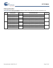
Changed TQFP package to Pb-free TQFP in Ordering Information section
Added BG Pb-free package
*B 333626
See ECN
SYT Modified Address Expansion balls in the pinouts for 100 TQFP and 119 BGA
Packages as per JEDEC standards and updated the Pin Definitions accordingly
Modified V
OL,
V
OH
test conditions
Replaced ‘Snooze’ with ‘Sleep’
Removed 117 MHz speed bin
Replaced TBDs for Θ
JA
and Θ
JC
to their respective values on the Thermal Resis-
tance table
Removed comment on the availability of BG Pb-free package
Updated the Ordering Information by shading and unshading MPNs as per
availability
*C 418633
See ECN
RXU Converted from Preliminary to Final
Changed address of Cypress Semiconductor Corporation on Page# 1 from
“3901 North First Street” to “198 Champion Court”
Modified test condition from V
IH
< V
DD
to
V
IH
< V
DD.
Modified test condition from V
DDQ
< V
DD
to V
DDQ
< V
DD
Modified Input Load to Input Leakage Current except ZZ and MODE in the
Electrical Characteristics Table
Replaced Package Name column with Package Diagram in the Ordering Infor-
mation table
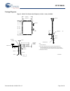
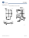
Replaced Package Diagram of 51-85050 from *A to *B
Updated the Ordering Information
*D 480124
See ECN
VKN Added the Maximum Rating for Supply Voltage on V
DDQ
Relative to GND
Updated the Ordering Information table.
*E 1274724
See ECN
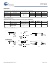
VKN Corrected Write Cycle timing waveform


