CY7C138, CY7C139
Document #: 38-06037 Rev. *D Page 2 of 17
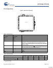
Pin Configurations
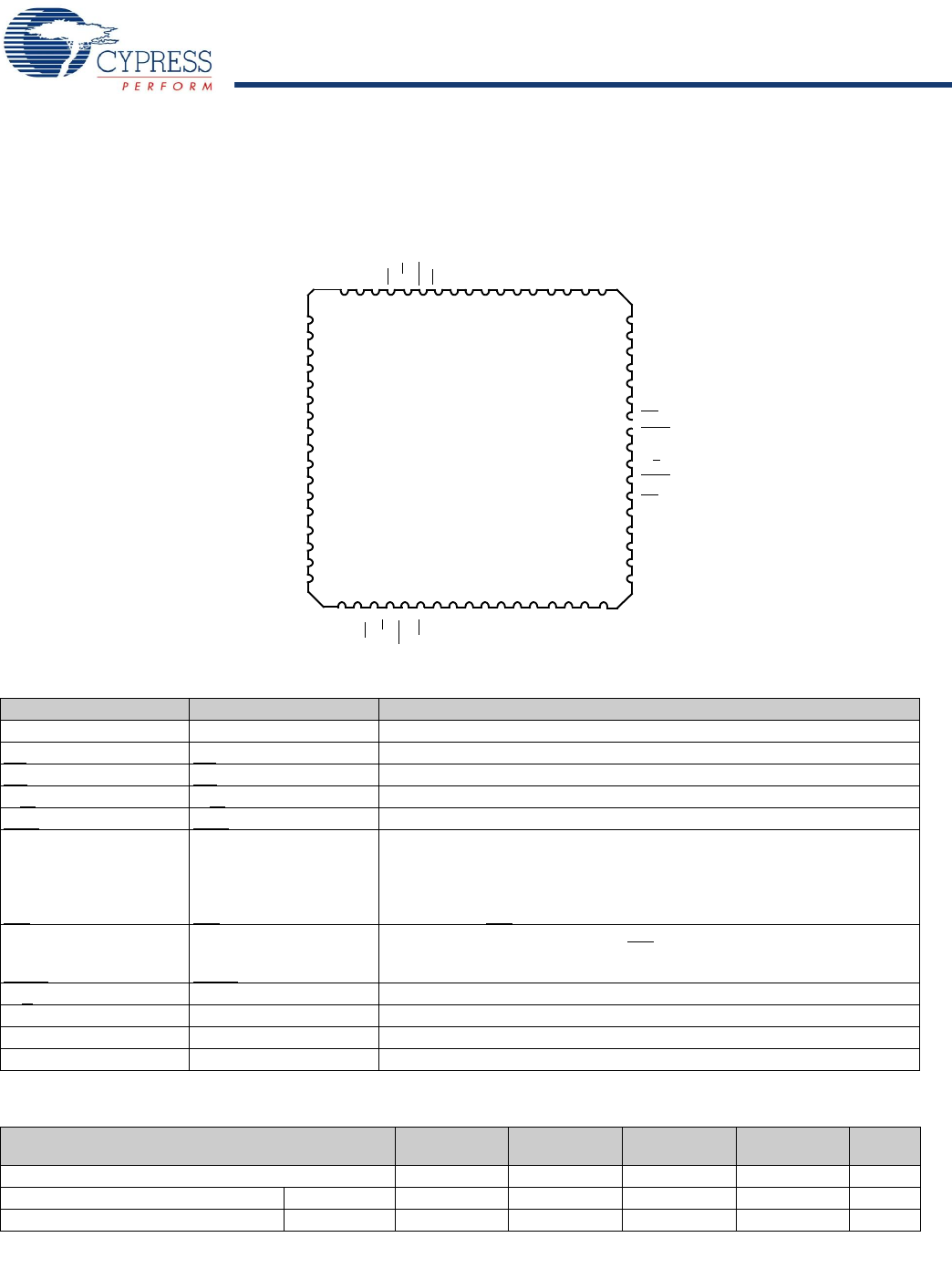
Figure 1. 68-Pin PLCC (Top View)
\
Table 1. Pin Definitions
Left Port Right Port Description
I/O
0L–7L(8L)
I/O
0R–7R(8R)
Data Bus Input/Output
A
0L–11L
A
0R–11R
Address Lines
CE
L
CE
R
Chip Enable
OE
L
OE
R
Output Enable
R/W
L
R/W
R
Read/Write Enable
SEM
L
SEM
R
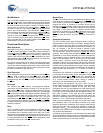
Semaphore Enable. When asserted LOW, allows access to eight
semaphores. The three least significant bits of the address lines will
determine which semaphore to write or read. The I/O
0
pin is used when
writing to a semaphore. Semaphores are requested by writing a 0 into the
respective location.
INT
L
INT
R
Interrupt Flag. INT
L
is set when right port writes location FFE and is cleared
when left port reads location FFE. INT
R
is set when left port writes location
FFF and is cleared when right port reads location FFF.
BUSY
L
BUSY
R
Busy Flag
M/S Master or Slave Select
V
CC
Power
GND Ground
10
11
12
13
14
15
16
17
18
19
20
21
22
23
24
67
60
59
58
57
56
55
54
53
52
51
50
49
48
3132 33 34 35 36 37 38 39 40 41 42 43
5 4 3 2 168 666564636261
A
A
4L
A
3L
A
2L
A
1L
A
0L
INT
L
BUSY
L
GND
M/S
BUSY
R
INT
R
A
0R
I/O
2L
I/O
3L
I/O
4L
I/O
5L
GND
I/O
6L
I/O
7L
V
CC
GND
I/O
0R
I/O
1R
I/O
2R
V
CC
A
2728 29 30
9876
47
46
45
44
A
1R
A
2R
A
3R
A
4R
I/O
3R
I/O
4R
I/O
5R
I/O
6R
25
26
6L
7L
A
8L
A
9L
A
A
10L
11L
V
CC
NC
NC
CE
L
SEM
L
R/W
L
OE
L
NC
I/O
I/O
1L
0L
A
A
6R
7R
A
8R
A
9R
A
10R
NC
NC
CE
R
SEM
R
R/W
R
OE
R
I/O
7R
GND
A
11R
A
5R
A
5L
NC
CY7C138/9
[3]
[4]
NC
NC
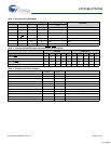
Table 2. Selection Guide
Description
7C138-15
7C139-15
7C138-25
7C139-25
7C138-35
7C139-35
7C138-55
7C139-55
Unit
Maximum Access Time (ns) 15 25 35 55 ns
Maximum Operating Current Commercial 220 180 160 160 mA
Maximum Standby Current for I
SB1
Commercial 60 40 30 30 mA
Notes
3. I/O
8R
on the CY7C139.
4. I/O
8L
on the CY7C139.
[+] Feedback


