CY7C1460AV25
CY7C1462AV25
CY7C1464AV25
Document #: 38-05354 Rev. *D Page 27 of 27
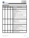
Document History Page
Document Title: CY7C1460AV25/CY7C1462AV25/CY7C1464AV25 36-Mbit (1-Mbit x 36/2-Mbit x 18/512K x 72) Pipelined
SRAM with NoBL™ Architecture
Document Number: 38-05354
REV. ECN No. Issue Date
Orig. of
Change Description of Change
** 254911 See ECN SYT New data sheet
Part number changed from previous revision (new and old part number
differ by the letter “A”)
*A 303533 See ECN SYT Changed H9 pin from V
SSQ
to V
SS
on the Pin Configuration table for 209
FBGA on Page # 5
Changed the test condition from V
DD
= Min. to V
DD
= Max for V
OL
in the
Electrical Characteristics table
Replaced Θ
JA
and Θ
JC
from TBD to respective Thermal Values for All
Packages on the Thermal Resistance Table
Changed I
DD
from 450, 400 & 350 mA to 435, 385 & 335 mA for 250, 200
and 167 Mhz respectively
Changed I
SB1
from 190, 180 and 170 mA to 185 mA for 250, 200 and 167
Mhz respectively
Changed I
SB2
from 80 mA to 100 mA for all frequencies
Changed I
SB3
from 180, 170 & 160 mA to 160 mA for 250, 200 and 167
Mhz respectively
Changed I
SB4
from 100 mA to 110 mA for all frequencies
Changed C
IN
, C
CLK
and C
I/O
to 6.5, 3 and 5.5 pF from 5, 5 and 7 pF for
TQFP Package
Changed t
CO
from 3.0 to 3.2 ns and t
DOH
from 1.3 ns to 1.5 ns for 200 Mhz
Speed Bin
Added lead-free information for 100 TQFP, 165 FBGA and 209 FBGA
packages
*B 331778 See ECN SYT Modified Address Expansion balls in the pinouts for 165 FBGA and 209
FBGA Package as per JEDEC standards and updated the Pin Definitions
accordingly
Modified V
OL,
V
OH
test conditions
Changed C
IN
, C
CLK
and C
I/O
to 7, 7and 6 pF from 5, 5 and 7 pF for 165
FBGA Package
Added Industrial Temperature Grade
Changed I
SB2
and I
SB4
from 100 and 110 mA to 120 and 135 mA respec-
tively
Updated the Ordering Information by Shading and Unshading MPNs as per
availability
*C 417547 See ECN RXU Converted from Preliminary to Final
Changed address of Cypress Semiconductor Corporation on Page# 1 from
“3901 North First Street” to “198 Champion Court”
Modified test condition from V
DDQ
< V
DD
to
V
DDQ
≤ V
DD
Changed I
X
current value in MODE from –5 & 30 µA to –30 & 5 µA respec-
tively and also Changed I
X
current value in ZZ from –30 & 5 µA to –5 & 30
µA respectively on page# 19
Modified “Input Load” to “Input Leakage Current except ZZ and MODE” in
the Electrical Characteristics Table
Replaced Package Name column with Package Diagram in the Ordering
Information table
Replaced Package Diagram of 51-85050 from *A to *B
*D 473650 See ECN VKN Added the Maximum Rating for Supply Voltage on V
DDQ
Relative to GND.
Changed t
TH
, t
TL
from 25 ns to 20 ns and t
TDOV
from 5 ns to 10 ns in TAP
AC Switching Characteristics table.
Updated the Ordering Information table.
[+] Feedback


