CY7C1460AV25
CY7C1462AV25
CY7C1464AV25
Document #: 38-05354 Rev. *D Page 9 of 27
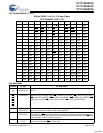
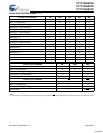
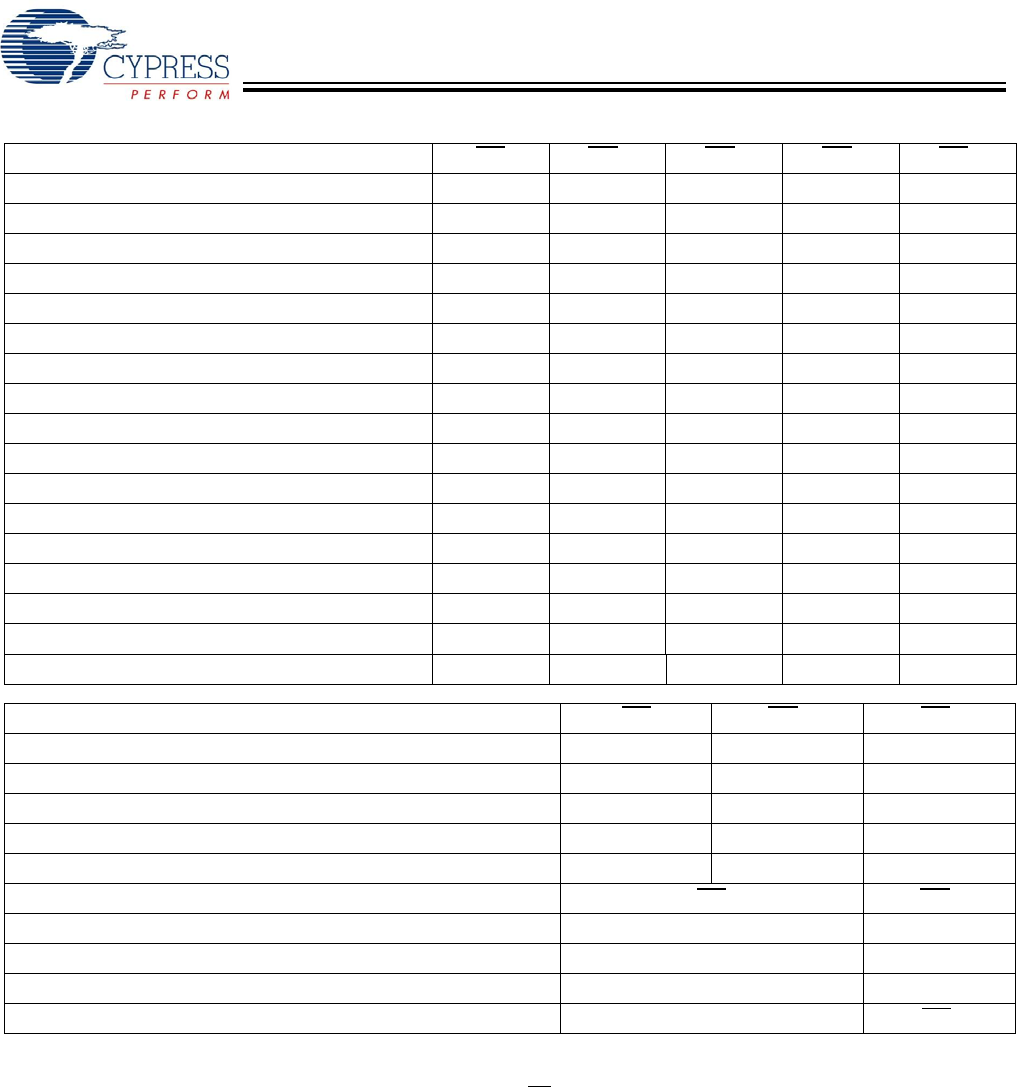
Partial Write Cycle Description
[1, 2, 3, 8]
Function (CY7C1460AV25) WE BW
d
BW
c
BW
b
BW
a
Read H X X X X
Write – No bytes written L H H H H
Write Byte a – (DQ
a
and
DQP
a
) LHHHL
Write Byte b – (DQ
b
and
DQP
b
)LHHLH
Write Bytes b, a L H H L L
Write Byte c – (DQ
c
and
DQP
c
)LHLHH
Write Bytes c, a L H L H L
Write Bytes c, b L H LL L H
Write Bytes c, b, a L H L L L
Write Byte d – (DQ
d
and
DQP
d
)LLHHH
Write Bytes d, a L L H H L
Write Bytes d, b LLHLH
Write Bytes d, b, a L L H L L
Write Bytes d, c L L L H H
Write Bytes d, c, a L L L H L
Write Bytes d, c, b L L L L H
Write All Bytes L L L L L
Function (CY7C1462AV25) WE BW
b
BW
a
Read H X X
Write – No Bytes Written L H H
Write Byte a – (DQ
a
and
DQP
a
)LHL
Write Byte b – (DQ
b
and
DQP
b
)LLH
Write Both Bytes L L L
Function (CY7C1464AV25) WE
BW
x
Read HX
Write – No Bytes Written L H
Write Byte X − (DQ
x
and
DQP
x)
LL
Write All Bytes LAll BW
= L
Note:
8. Table only lists a partial listing of the byte write combinations. Any combination of BW
X
is valid. Appropriate write will be done based on which byte write is active.
[+] Feedback


