CY7C1470BV33
CY7C1472BV33, CY7C1474BV33
Document #: 001-15031 Rev. *C Page 21 of 30
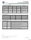
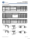
I
SB3
Automatic CE
Power Down
Current—CMOS Inputs
Max. V
DD
, Device Deselected,
V
IN
≤ 0.3V or V
IN
> V
DDQ
− 0.3V,
f = f
MAX
= 1/t
CYC
4.0-ns cycle, 250 MHz 245 mA
5.0-ns cycle, 200 MHz 245 mA
6.0-ns cycle, 167 MHz 245 mA
I
SB4
Automatic CE
Power Down
Current—TTL Inputs
Max. V
DD
, Device Deselected,
V
IN
≥ V
IH
or V
IN
≤ V
IL
, f = 0
All speed grades 135 mA
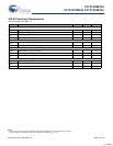
Capacitance
Tested initially and after any design or process changes that may affect these parameters.
Parameter Description Test Conditions
100 TQFP
Max
165 FBGA
Max
209 FBGA
Max
Unit
C
ADDRESS
Address Input Capacitance T
A
= 25°C, f = 1 MHz,
V
DD
= 3.3V
V
DDQ
= 2.5V
6 6 6 pF
C
DATA
Data Input Capacitance 5 5 5 pF
C
CTRL
Control Input Capacitance 8 8 8 pF
C
CLK
Clock Input Capacitance 6 6 6 pF
C
IO
Input/Output Capacitance 5 5 5 pF
Thermal Resistance
Tested initially and after any design or process changes that may affect these parameters.
Parameters Description Test Conditions
100 TQFP
Package
165 FBGA
Package
209 FBGA
Package
Unit
Θ
JA
Thermal Resistance
(Junction to Ambient)
Test conditions follow standard
test methods and procedures for
measuring thermal impedance,
per EIA/JESD51.
24.63 16.3 15.2 °C/W
Θ
JC
Thermal Resistance
(Junction to Case)
2.28 2.1 1.7 °C/W
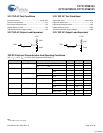
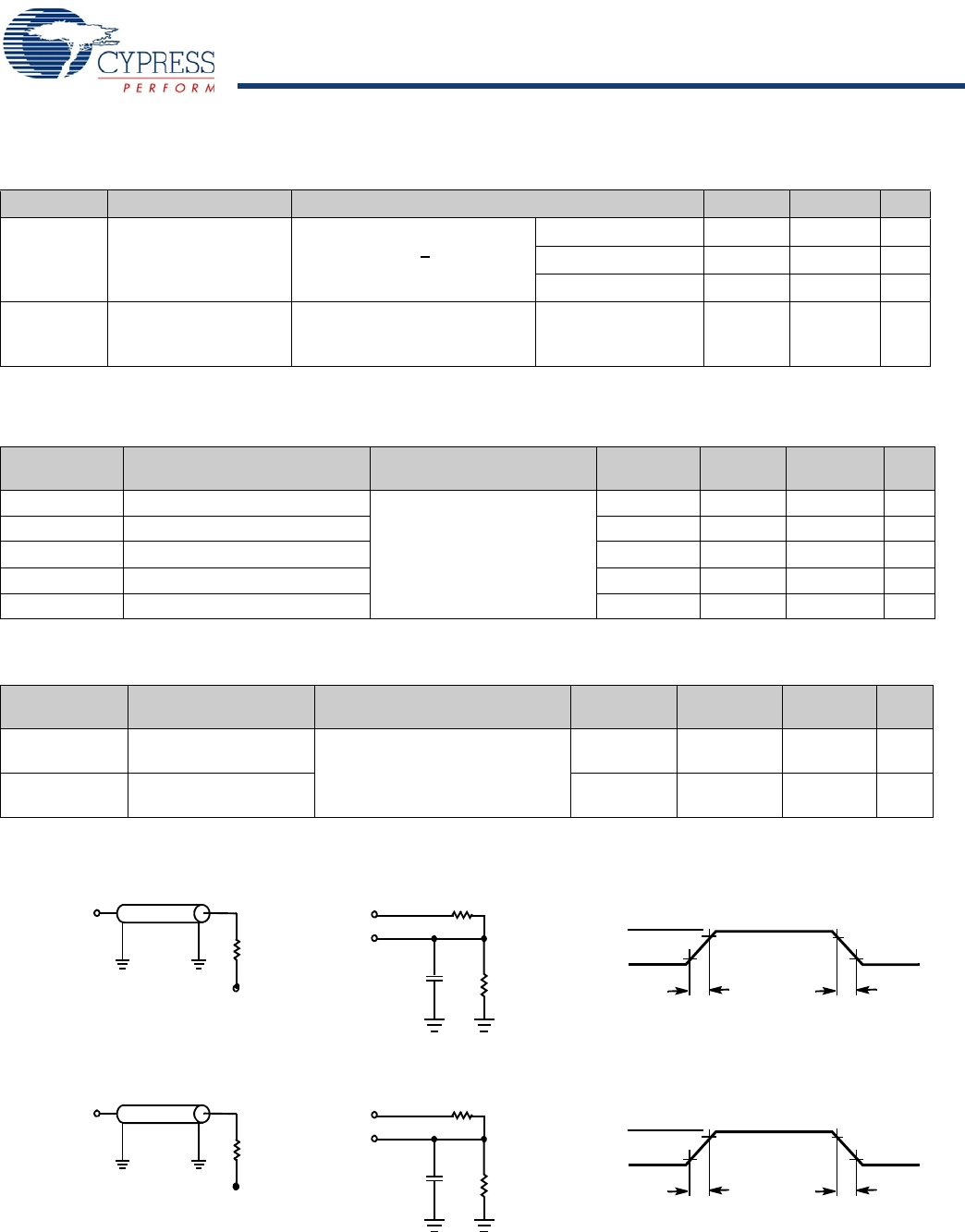
AC Test Loads and Waveforms
Electrical Characteristics
Over the Operating Range
[13, 14]
(continued)
Parameter Description Test Conditions Min Max Unit
OUTPUT
R = 317Ω
R = 351Ω
5pF
INCLUDING
JIG AND
SCOPE
(a)
(b)
OUTPUT
R
L
= 50Ω
Z
0
= 50Ω
V
L
= 1.5V
3.3V
ALL INPUT PULSES
V
DDQ
GND
90%
10%
90%
10%
≤ 1 ns
≤ 1 ns
(c)
3.3V IO Test Load
OUTPUT
R = 1667Ω
R = 1538Ω
5pF
INCLUDING
JIG AND
SCOPE
(a)
(b)
OUTPUT
R
L
= 50Ω
Z
0
= 50Ω
V
L
= 1.25V
2.5V
ALL INPUT PULSES
V
DDQ
GND
90%
10%
90%
10%
≤ 1 ns
≤ 1 ns
(c)
2.5V IO Test Load
[+] Feedback


