CY7C1470BV33
CY7C1472BV33, CY7C1474BV33
Document #: 001-15031 Rev. *C Page 11 of 30
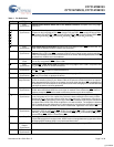
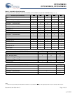
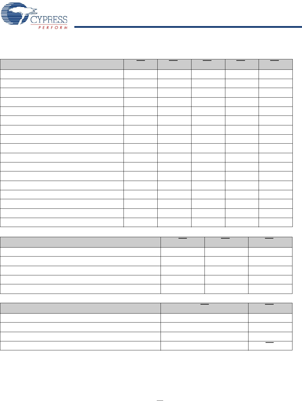
Table 5. Partial Write Cycle Description
The partial write cycle description for CY7C1470BV33, CY7C1472BV33, and CY7C1474BV33 follows.
[1, 2, 3, 8]
Function (CY7C1470BV33) WE BW
d
BW
c
BW
b
BW
a
Read H X X X X
Write – No bytes written L H H H H
Write Byte a – (DQ
a
and
DQP
a
)LHHHL
Write Byte b – (DQ
b
and
DQP
b
)LHHLH
Write Bytes b, a L H H L L
Write Byte c – (DQ
c
and
DQP
c
)LHLHH
Write Bytes c, a L H L H L
Write Bytes c, b L H L L H
Write Bytes c, b, a L H L L L
Write Byte d – (DQ
d
and
DQP
d
) LLHHH
Write Bytes d, a L L H H L
Write Bytes d, b L L H L H
Write Bytes d, b, a L L H L L
Write Bytes d, c L L L H H
Write Bytes d, c, a L L L H L
Write Bytes d, c, b L L L L H
Write All Bytes L L L L L
Function (CY7C1472BV33) WE BW
b
BW
a
Read Hxx
Write – No Bytes Written L H H
Write Byte a – (DQ
a
and
DQP
a
)LHL
Write Byte b – (DQ
b
and
DQP
b
)LLH
Write Both Bytes L L L
Function (CY7C1474BV33) WE BW
x
Read Hx
Write – No Bytes Written L H
Write Byte X − (DQ
x
and
DQP
x)
LL
Write All Bytes L All BW
= L
Note
8. Table lists only a partial listing of the Byte Write combinations. Any combination of BW
[a:d]
is valid. Appropriate Write is based on which Byte Write is active.
[+] Feedback


