CY7C63413C
CY7C63513C
CY7C63613C
Document #: 38-08027 Rev. *B Page 9 of 32
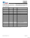
I/O Register Summary
I/O registers are accessed via the I/O Read (IORD) and I/O
Write (IOWR, IOWX) instructions. IORD reads the selected
port into the accumulator. IOWR writes data from the accumu-
lator to the selected port. Indexed I/O Write (IOWX) adds the
contents of X to the address in the instruction to form the port
address and writes data from the accumulator to the specified
port. Note that specifying address 0 (e.g., IOWX 0h) means
the I/O port is selected solely by the contents of X.
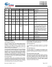
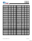
Table 1. I/O Register Summary
Register Name I/O Address Read/Write Function
Port 0 Data 0x00 R/W GPIO Port 0
Port 1 Data 0x01 R/W GPIO Port 1
Port 2 Data 0x02 R/W GPIO Port 2
Port 3 Data 0x03 R/W GPIO Port 3
Port 0 Interrupt Enable 0x04 W Interrupt enable for pins in Port 0
Port 1 Interrupt Enable 0x05 W Interrupt enable for pins in Port 1
Port 2 Interrupt Enable 0x06 W Interrupt enable for pins in Port 2
Port 3 Interrupt Enable 0x07 W Interrupt enable for pins in Port 3
GPIO Configuration 0x08 R/W GPIO Ports Configurations
USB Device Address A 0x10 R/W USB Device Address A
EP A0 Counter Register 0x11 R/W USB Address A, Endpoint 0 counter register
EP A0 Mode Register 0x12 R/W USB Address A, Endpoint 0 configuration register
EP A1 Counter Register 0x13 R/W USB Address A, Endpoint 1 counter register
EP A1 Mode Register 0x14 R/C USB Address A, Endpoint 1 configuration register
EP A2 Counter Register 0x15 R/W USB Address A, Endpoint 2 counter register
EP A2 Mode Register 0x16 R/C USB Address A, Endpoint 2 configuration register
USB Status & Control 0x1F R/W USB upstream port traffic status and control register
Global Interrupt Enable 0x20 R/W Global interrupt enable register
Endpoint Interrupt Enable 0x21 R/W USB endpoint interrupt enables
Timer (LSB) 0x24 R Lower eight bits of free-running timer (1 MHz)
Timer (MSB) 0x25 R Upper four bits of free-running timer that are latched
when the lower eight bits are read.
WDR Clear 0x26 W Watch Dog Reset clear
DAC Data 0x30 R/W DAC I/O
[2]
DAC Interrupt Enable 0x31 W Interrupt enable for each DAC pin
DAC Interrupt Polarity 0x32 W Interrupt polarity for each DAC pin
DAC Isink 0x38-0x3F W One four bit sink current register for each DAC pin
Processor Status & Control 0xFF R/W Microprocessor status and control
Note:
2. DAC I/O Port not bonded out on CY7C63613C. See note on page 12 for firmware code needed for unused GPIO pins.
[+] Feedback


