CY7C68013A, CY7C68014A
CY7C68015A, CY7C68016A
Document #: 38-08032 Rev. *L Page 23 of 62
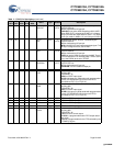
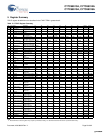
85 70 43 36 7F PA3 or
WU2
IO/Z I
(PA3)
Multiplexed pin whose function is selected by:
WAKEUP.7 and OEA.3
PA3 is a bidirectional IO port pin.
WU2 is an alternate source for USB Wakeup, enabled
by WU2EN bit (WAKEUP.1) and polarity set by
WU2POL (WAKEUP.4). If the 8051 is in suspend and
WU2EN = 1, a transition on this pin starts up the oscil-
lator and interrupts the 8051 to enable it to exit the
suspend mode. Asserting this pin inhibits the chip from
suspending, if WU2EN = 1.
89 71 44 37 6F PA4 or
FIFOADR0
IO/Z I
(PA4)
Multiplexed pin whose function is selected by:
IFCONFIG[1..0].
PA4 is a bidirectional IO port pin.
FIFOADR0 is an input-only address select for the slave
FIFOs connected to FD[7..0] or FD[15..0].
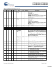
90 72 45 38 8C PA5 or
FIFOADR1
IO/Z I
(PA5)
Multiplexed pin whose function is selected by:
IFCONFIG[1..0].
PA5 is a bidirectional IO port pin.
FIFOADR1 is an input-only address select for the slave
FIFOs connected to FD[7..0] or FD[15..0].
91 73 46 39 7C PA6 or
PKTEND
IO/Z I
(PA6)
Multiplexed pin whose function is selected by the
IFCONFIG[1:0] bits.
PA6 is a bidirectional IO port pin.
PKTEND is an input used to commit the FIFO packet
data to the endpoint and whose polarity is program-
mable via FIFOPINPOLAR.5.
92 74 47 40 6C PA7 or
FLAGD or
SLCS#
IO/Z I
(PA7)
Multiplexed pin whose function is selected by the
IFCONFIG[1:0] and PORTACFG.7 bits.
PA7 is a bidirectional IO port pin.
FLAGD is a programmable slave-FIFO output status
flag signal.
SLCS# gates all other slave FIFO enable/strobes
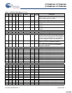
Port B
44 34 25 18 3H PB0 or
FD[0]
IO/Z I
(PB0)
Multiplexed pin whose function is selected by the
following bits: IFCONFIG[1..0].
PB0 is a bidirectional IO port pin.
FD[0] is the bidirectional FIFO/GPIF data bus.
45 35 26 19 4F PB1 or
FD[1]
IO/Z I
(PB1)
Multiplexed pin whose function is selected by the
following bits: IFCONFIG[1..0].
PB1 is a bidirectional IO port pin.
FD[1] is the bidirectional FIFO/GPIF data bus.
46 36 27 20 4H PB2 or
FD[2]
IO/Z I
(PB2)
Multiplexed pin whose function is selected by the
following bits: IFCONFIG[1..0].
PB2 is a bidirectional IO port pin.
FD[2] is the bidirectional FIFO/GPIF data bus.
47 37 28 21 4G PB3 or
FD[3]
IO/Z I
(PB3)
Multiplexed pin whose function is selected by the
following bits: IFCONFIG[1..0].
PB3 is a bidirectional IO port pin.
FD[3]
is the bidirectional FIFO/GPIF data bus.
54 44 29 22 5H PB4 or
FD[4]
IO/Z I
(PB4)
Multiplexed pin whose function is selected by the
following bits: IFCONFIG[1..0].
PB4 is a bidirectional IO port pin.
FD[4] is the bidirectional FIFO/GPIF data bus.
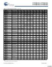
Table 11. FX2LP Pin Descriptions (continued)
128
TQFP
100
TQFP
56
SSOP
56
QFN
56 VF-
BGA
Name Type Default Description
[+] Feedback [+] Feedback


