CY7C68013A, CY7C68014A
CY7C68015A, CY7C68016A
Document #: 38-08032 Rev. *L Page 2 of 62
1.1 Features (CY7C68013A/14A only)
■ CY7C68014A: Ideal for battery powered applications
❐ Suspend current: 100 μA (typ)
■ CY7C68013A: Ideal for non-battery powered applications
❐ Suspend current: 300 μA (typ)
■ Available in five lead-free packages with up to 40 GPIOs
❐ 128-pin TQFP (40 GPIOs), 100-pin TQFP (40 GPIOs), 56-pin
QFN (24 GPIOs), 56-pin SSOP (24 GPIOs), and 56-pin VF-
BGA (24 GPIOs)
1.2 Features (CY7C68015A/16A only)
■ CY7C68016A: Ideal for battery powered applications
❐ Suspend current: 100 μA (typ)
■ CY7C68015A: Ideal for non-battery powered applications
❐ Suspend current: 300 μA (typ)
■ Available in lead-free 56-pin QFN package (26 GPIOs)
❐ 2 more GPIOs than CY7C68013A/14A enabling additional
features in same footprint
Cypress Semiconductor Corporation’s (Cypress’s) EZ-USB
FX2LP™ (CY7C68013A/14A) is a low power version of the
EZ-USB FX2™ (CY7C68013), which is a highly integrated, low
power USB 2.0 microcontroller. By integrating the USB 2.0 trans-
ceiver, serial interface engine (SIE), enhanced 8051 microcon-
troller, and a programmable peripheral interface in a single chip,
Cypress has created a cost effective solution that provides
superior time-to-market advantages with low power to enable
bus powered applications.
The ingenious architecture of FX2LP results in data transfer
rates of over 53 Mbytes per second, the maximum allowable
USB 2.0 bandwidth, while still using a low cost 8051 microcon-
troller in a package as small as a 56 VFBGA (5mm x 5mm).
Because it incorporates the USB 2.0 transceiver, the FX2LP is
more economical, providing a smaller footprint solution than
USB 2.0 SIE or external transceiver implementations. With
EZ-USB FX2LP, the Cypress Smart SIE handles most of the
USB 1.1 and 2.0 protocol in hardware, freeing the embedded
microcontroller for application specific functions and decreasing
development time to ensure USB compatibility.
The General Programmable Interface (GPIF) and Master/Slave
Endpoint FIFO (8-bit or 16-bit data bus) provides an easy and
glueless interface to popular interfaces such as
ATA, UTOPIA,
EPP, PCMCIA, and most DSP/processors.
The FX2LP draws less current than the FX2 (CY7C68013), has
double the on-chip code/data RAM, and is fit, form and function
compatible with the 56, 100, and 128 pin FX2.
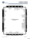
Five packages are defined for the family: 56VFBGA, 56 SSOP,
56 QFN, 100 TQFP, and 128 TQFP.
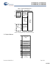
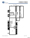
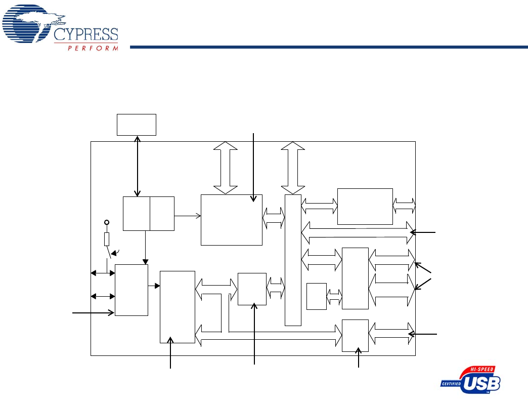
Address (16)
x20
PLL
/0.5
/1.0
/2.0
8051 Core
12/24/48 MHz,
four clocks/cycle
I
2
C
VCC
1.5k
D+
D–
Address (16) / Data Bus (8)
FX2LP
GPIF
CY
Smart
USB
1.1/2.0
Engine
USB
2.0
XCVR
16 KB
RAM
4 kB
FIFO
Integrated
full-speed and
Additional IOs (24)
ADDR (9)
CTL (6)
RDY (6)
8/16
Data (8)
24 MHz
Ext. XTAL
Enhanced USB core
Simplifies 8051 code
“Soft Configuration”
Easy firmware changes
FIFO and endpoint memory
(master or slave operation)
Up to 96 MBytes/s
burst rate
General
programmable I/F
to ASIC/DSP or bus
standards such as
ATAPI, EPP, etc.
Abundant IO
including two USARTS
High performance micro
using standard tools
with lower-power options
Master
connected for
full-speed
ECC
XCVR
high-speed
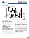
Logic Block DiagramLogic Block Diagram
[+] Feedback [+] Feedback


