CY7C68033/CY7C68034
Document #: 001-04247 Rev. *D Page 14 of 33
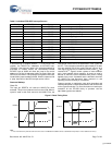
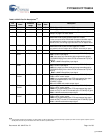
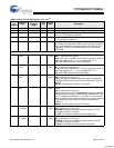
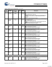
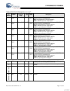
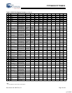
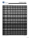
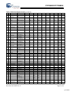
Table 8. NX2LP-Flex Pin Descriptions
[6]
56 QFN
Pin
Number
Default Pin
Name
NAND
Firmware
Usage
Pin
Type
Default
State
Description
9 DMINUS N/A I/O/Z Z USB D– Signal. Connect to the USB D– signal.
8 DPLUS N/A I/O/Z Z USB D+ Signal. Connect to the USB D+ signal.
42 RESET# N/A Input N/A Active LOW Reset. Resets the entire chip. See section ”Reset and
Wakeup” on page 7 for more details.
5 XTALIN N/A Input N/A Crystal Input. Connect this signal to a 24-MHz parallel-resonant,
fundamental mode crystal and load capacitor to GND.
It is also correct to drive XTALIN with an external 24-MHz square
wave derived from another clock source. When driving from an
external source, the driving signal should be a 3.3V square wave.
4 XTALOUT N/A Output N/A Crystal Output. Connect this signal to a 24-MHz parallel-resonant,
fundamental mode crystal and load capacitor to GND.
If an external clock is used to drive XTALIN, leave this pin open.
54 GPIO9 GPIO9 O/Z 12 MHz GPIO9 is a bidirectional IO port pin.
1 RDY0 or
SLRD
R_B1# Input N/A Multiplexed pin whose function is selected by IFCONFIG[1:0].
RDY0 is a GPIF input signal.
SLRD is the input-only read strobe with programmable polarity
(FIFOPINPOLAR[3]) for the slave FIFOs connected to FD[7:0] or
FD[15:0].
R_B1# is a NAND Ready/Busy input signal.
2 RDY1 or
SLWR
R_B2# Input N/A Multiplexed pin whose function is selected by IFCONFIG[1:0].
RDY1 is a GPIF input signal.
SLWR is the input-only write strobe with programmable polarity
(FIFOPINPOLAR[2]) for the slave FIFOs connected to FD[7:0] or
FD[15:0].
R_B2# is a NAND Ready/Busy input signal.
29 CTL0 or
FLAGA
WE# O/Z H Multiplexed pin whose function is selected by IFCONFIG[1:0].
CTL0 is a GPIF control output.
FLAGA is a programmable slave-FIFO output status flag signal.
Defaults to programmable for the FIFO selected by the
FIFOADR[1:0] pins.
WE# is the NAND write enable output signal.
30 CTL1 or
FLAGB
RE0# O/Z H Multiplexed pin whose function is selected by IFCONFIG[1:0].
CTL1 is a GPIF control output.
FLAGB is a programmable slave-FIFO output status flag signal.
Defaults to FULL for the FIFO selected by the FIFOADR[1:0] pins.
RE0# is a NAND read enable output signal.
31 CTL2 or
FLAGC
RE1# O/Z H Multiplexed pin whose function is selected by IFCONFIG[1:0].
CTL2 is a GPIF control output.
FLAGC is a programmable slave-FIFO output status flag signal.
Defaults to EMPTY for the FIFO selected by the FIFOADR[1:0] pins.
RE1# is a NAND read enable output signal.
Note
6. Unused inputs should not be left floating. Tie either HIGH or LOW as appropriate. Outputs should only be pulled up or down to ensure signals at power-up and i
n
standby. Note also that no pins should be driven while the device is powered down.
[+] Feedback


