CY7C68300C/CY7C68301C
CY7C68320C/CY7C68321C
Document 001-05809 Rev. *A Page 20 of 42
MfgCB
The mfg_load and mfg_read vendor-specific commands are
passed down through the bulk pipe in the CBWCB portion of
the CBW. The format of this MfgCB is shown as follows. Byte0
is a vendor-specific command designator whose value is
configurable and set in the AT2LP configuration data. Byte 1
must be 0x27 to identify a MfgCB. Bytes 2 through 15 are
reserved and must be set to zero.
The data transfer length is determined by the CBW Data
Transfer Length specified in bytes 8 through 11
(dCBWDataTransferLength) of the CBW. The type and
direction of the command is determined by the direction bit
specified in byte 12, bit 7 (bmCBWFlags) of the CBW.
Mfg_load
During a Mfg_load, the AT2LP enters into Manufacturing Test
Mode. Manufacturing Test Mode is provided as a means to
implement board or system level interconnect tests. During
Manufacturing Test Mode operation, all outputs not directly
associated with USB operation are controllable. Normal
control of the output pins are disabled. Control of the select
AT2LP IO pins and their tri-state controls are mapped to the
ATAPI data packet associated with this request. (See Table 10
for an explanation of the required Mfg_load data format.) Any
data length can be specified, but only bytes 0 through 3 are
mapped to pins, so a length of 4 bytes is recommended. To
exit Manufacturing Test Mode, a hard reset (toggle RESET#)
is required.
Mfg_read
This USB request returns a ’snapshot’ of select AT2LP input
pins. AT2LP input pins not directly associated with USB
operation can be sampled at any time during Manufacturing
Test Mode operation. See Table 10 for an explanation of the
Mfg_read data format. Any data length can be specified, but
only bytes 0 through 3 contain usable information, so a length
of 4 bytes is recommended.
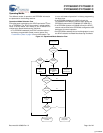
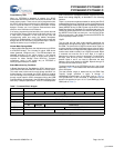
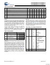
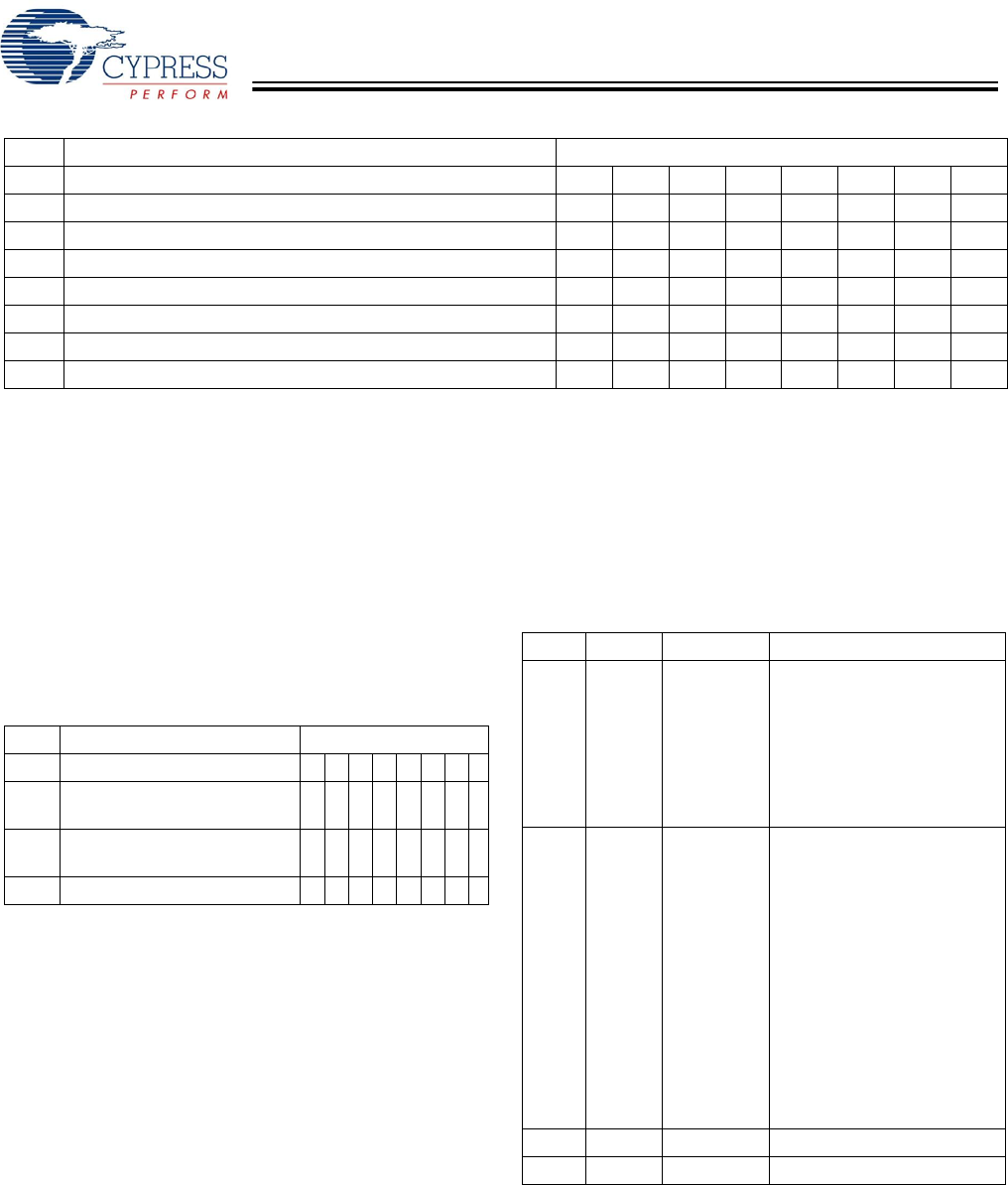
Table 8. Example CfgCB
Offset CfgCB Byte Descriptions Bits
76543210
0 bVSCBSignature (set in configuration bytes) 00100100
1 bVSCBSubCommand (must be 0x26) 00100110
2 Reserved (must be set to zero) 00000000
3 Data Source (must be set to 0x02) 00000010
4 Start Address (LSB) (must be set to zero) 00000000
5 Start Address (MSB) (must be set to zero) 00000000
6–15 Reserved (must be set to zero) 00000000
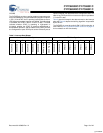
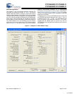
Table 9. Example MfgCB
Offset MfgCB Byte Description Bits
76543210
0 0 bVSCBSignature
(set in configuration bytes)
00100100
1 1 bVSCBSubCommand
(hardcoded 0x27)
00100111
2–15 2–15 Reserved (must be zero) 0 0 0 0 0 0 0 0
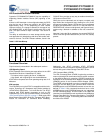
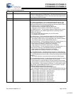
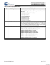
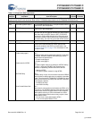
Table 10.Mfg_read and Mfg_load Data Format
Byte Bits Read/Load Function
0 7 R/L ARESET#
6RDA2
5:4 R/L CS#[1:0]
3 R/L DRVPWRVLD
2:1 R/L DA[1:0]
0RINTRQ
1 7 L DD[15:0] High-Z Status
0 = Hi-Z all DD pins
1 = Drive DD pins
6RMFG_SEL
0 = Mass Storage Mode
1 = Manufacturing Mode
5 R VBUS_ATA_ENABLE
4RDMARQ
3 R IORDY
2R/LDMACK#
1R/LDIOR#
0R/LDIOW#
2 7:0 R/L DD[7:0]
3 7:0 R/L DD[15:8]
[+] Feedback


