CY8C21634, CY8C21534
CY8C21434, CY8C21334, CY8C21234
Document Number: 38-12025 Rev. *O Page 23 of 45
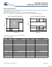
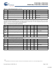
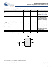
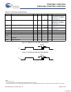
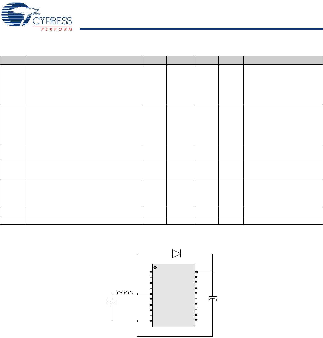
Figure 15. Basic Switch Mode Pump Circuit
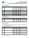
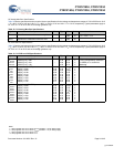
ΔV
PUMP_
Line
Line Regulation (over Vi range) – 5 – %V
O
Configuration of footnote.
[6]
V
O
is the “Vdd Value for PUMP
Trip” specified by the VM[2:0]
setting in the DC POR and LVD
Specification, Table 23 on page
24.
ΔV
PUMP_
Load
Load Regulation – 5 – %V
O
Configuration of footnote.
[6]
V
O
is the “Vdd Value for PUMP
Trip” specified by the VM[2:0]
setting in the DC POR and LVD
Specification, Table 23 on page
24.
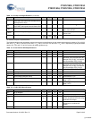
ΔV
PUMP_
Ripple
Output Voltage Ripple (depends on cap/load) – 100 – mVpp Configuration of footnote.
[6]
Load is 5 mA.
E
3
Efficiency 35 50 – % Configuration of footnote.
[6]
Load is 5 mA. SMP trip voltage
is set to 3.25V.
E
2
Efficiency 35 80 – % For I load = 1mA, V
PUMP
=
2.55V, V
BAT
= 1.3V,
10 uH inductor, 1 uF capacitor,
and Schottky diode.
F
PUMP
Switching Frequency – 1.3 – MHz
DC
PUMP
Switching Duty Cycle – 50 – %
Table 21. DC Switch Mode Pump (SMP) Specifications (continued)
Symbol Description Min Typ Max Units Notes
Battery
C1
D1
+
PSoC
Vdd
Vss
SMP
V
BAT
L
1
V
PUMP
Note
6. L
1
= 2 mH inductor, C
1
= 10 mF capacitor, D
1
= Schottky diode. See Figure 15.
[+] Feedback


