


November 21, 2002 Document No. 001-43117 Rev. ** 3
AN1196
Maintain PCB Trace Impedance
Designing the PCB traces for particular characteristic imped-
ance is very important to signal quality. The USB specification
requires controlled impedance among all elements in the
USB data path. The differential impedance of each USB data
pair should be 90 ohms with a 10% tolerance to match the
differential output impedance of high-speed capable drivers.
A common way to implement a differential pair is to use an
edge-coupled, surface micro-strip line. The pair is placed on
the board’s surface layer, and is directly over a ground plane
layer. This is the scenario used in the design of the CY4611.
The following five parameters set the value for the differential
impedance.
Parameters h, t, w, and s may be any unit but must be con-
sistent. For example, the CY4611 design referenced in this
application note shows these units in mil, (an English unit,
1/1000th of an inch).
ε
r
is a dimensionless constant.
For an edge-coupled, surface micro-strip, these five parame-
ters (h,
ε
r
, t, w, and s) set the value for the differential imped-
ance (“Zdiff”). Zdiff is defined in terms of the impedance of
each line of the pair, (“Z
0
”). The equations approximating
impedance are:
Equation 1
Equation 2
The above equations yield a good estimate of Z
0
and Zdiff
when the following conditions are true:
The reference section lists a book resource and cites a URL
for downloading a spreadsheet for calculating the imped-
ances mentioned. The following is an example of calculating
the trace impedance that is used in the CY4611 FX2 USB to
ATA/CF Reference Design.
Table 3, which is extracted from the CY4611 FX2 USB to
ATA/CF Reference Design drawings, shows the dimensions
that impact the impedance for the USB data traces. These
dimensions must not only satisfy the required characteristic
impedance but must also be applicable in a practical physical
design. For instance, different fabrication processes may
have limited choices for material dielectric constant and
material thickness between the signal layer and the ground
layer. These two parameters dictate the trace dimensions for
this design. The PCB manufacturer's material for the PCB
was taken from their standard supply. The vendor provided
the tolerance values shown in Table 3. The values are all fin-
ished dimensions.
Using the dimensions from Table 3, the Zdiff for the USB
data pairs of the CY4611 FX2 USB to ATA/CF Reference
Design is 90 ohms +0%, –4%.
The designer should take advantage of any help available
from the PCB manufacturer. The key dimensions and toler-
ances should be available from the manufacturer. Some
manufacturers will perform the impedance calculations for the
designer. Some will provide a service to measure the imped-
ance after the PCB is fabricated.
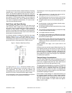
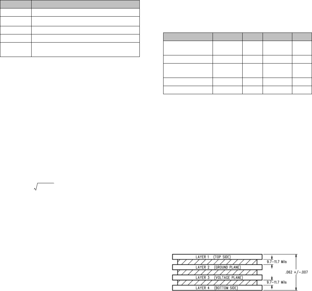
PCB Layer Stack-Up
For best signal characteristics, a USB 2.0 high-speed design
requires at least a four-layer PCB. It is recommended to
place the primary components (CY7C68013 and its crystal)
on the first (or top) layer, followed by the solid signal ground
plane. The third layer should be the voltage plane followed by
the fourth bottom layer. Figure 3 below illustrates these 4 lay-
ers which are used in the PCB for the CY4611 FX2 USB to
ATA/CF Reference Design.
Figure 3. Recommended PCB Stack-up
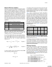
Table 2. Parameters for Differential Impedence
Term Description
h Height of signal traces above ground plane
ε
r
Material dielectric constant
t Trace thickness
wTrace width
s Spacing between each trace of a differential
pair, inside edge-to-edge
Zdiff 2 Z
0
10.48– e
0.96–
s
h
---
⋅
⋅
⎝⎠
⎜⎟
⎛⎞
ohms⋅⋅=
Z
0
87
ε
r 1.41+
----------------------
⎝⎠
⎛⎞
In
5.98 h⋅
0.8 wt+⋅
------------------------
⎝⎠
⎛⎞
ohms⋅=
w
h
----
⎝⎠
⎛⎞
2.0≤
0.20
s
h
---
⎝⎠
⎛⎞
3.0≤≤
Table 3. Tolerance Values
Tolerances Min. Nominal Max.
Material Thick-
ness(mils)
±1.0 9.7 10.7 11.7
Material Dielectric ±0.2 3.8 4.0 4.2
Trace Thickness,
1 oz. (mils)
±0.1 2.3 2.4 2.5
Width (mils) ±0.5 16.75 17.25 17.75
Spacing (mils) ±1.0 12.75 13.75 14.75
[+] Feedback [+] Feedback