


November 21, 2002 Document No. 001-43117 Rev. ** 5
AN1196
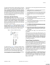
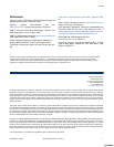
The design of the land area for the exposed paddle is critical
to proper thermal transfer. A copper fill is to be designed into
the PCB and under the QFN in order to assist thermal trans-
fer. Figure 5 is the diagram of the PCB land area for the EZ-
USB FX2.
Figure 5. Diagram of the PCB Land Area
The heat is transferred to the solid signal ground plane of the
board. The connection is made using a 5 x 5 array of 25
plated through-holes in the PCB; each should have a finished
diameter ranging from 12 mil to 13 mil. Solder mask is placed
over the top of each plated through-hole to resist solder flow
into the hole. The mask also is used to create voids in the
flowed solder for out-gassing during the solder reflow pro-
cess.
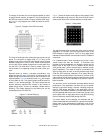
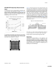
Research done by Amkor, a package manufacturer, has
determined that an array of more than 16 and less than 36
plated through-holes should be used for the PCB land for the
exposed paddle. Figure 6 shows the trend in Θ
ja
with respect
to the number of vias. This specific graph show the trend on
Amkor’s 7 mm 48-lead package. The result shows that the
thermal efficiency improves with increase in the number of
plated though holes. A lower Θ
ja
indicates a better thermal
efficiency. The results obtained on the Amkor part can be
extrapolated to the EZ-USB FX2.
Figure 6. Thermal Efficiency
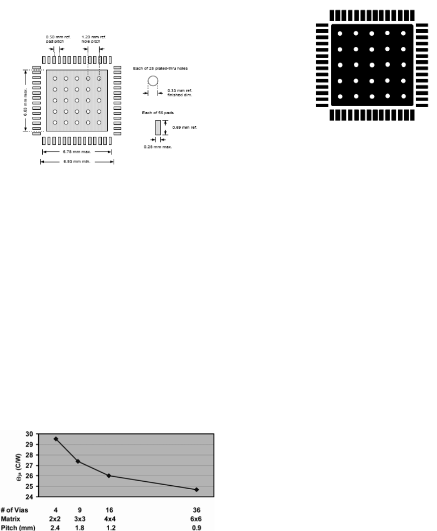
Figure 7 shows the solder mask region at the package. Each
of the 25 plated through-holes is in the center of each circle of
solder mask. Black area indicates absence of solder mask.
Figure 7. Solder Mask
The signal ground plane provides the major area for thermal
dissipation. The CY4611 uses the large internal layer of the
PCB devoted to signal ground. This is a fairly large board
intended for demonstration and evaluation of the CY7C68013
component.
For a fielded product, some developers may need a much
smaller board size than the CY4611. To maximize area
devoted to thermal dissipation, the designer should use the
bottom layer of the PCB. This is in addition to the internal
solid ground plane, (which must be kept to maintain proper
signal impedance). The metal fill must be connected to the
signal ground plane at each of the 25 plated through-holes
under the QFN mounting. Additional 13-mil plated through-
holes may be placed throughout the board to connect to the
internal signal ground plane as desired. Most holes should be
placed as close to the QFN package as practical to improve
thermal transfer.
The enclosure for the circuit board assembly affects thermal
performance. This application note does not give a specific
example of enclosure design. However, following the guide-
lines for PCB design described in this application note will
assure the most efficient method to conduct heat away from
the QFN package without the use of heat sinks. A large, solid
ground plane with no large gaps close to the QFN mounting
area will efficiently conduct heat through the PCB.
For further details on this package and methods and pro-
cesses associated with its assembly to a printed circuit board,
please refer to the manufacturer's application note for the
package. It is identified in the References section of this doc-
ument.
[+] Feedback [+] Feedback