


SFBD-1250B4Q1R
DELTA ELECTRONICS, INC.
4 Revision: S0
04/12/2007
www.deltaww.com
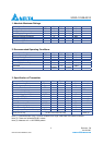
Note (1). A (TX)+ B (RX) = 300mA (Not include termination circuit)
Note (2). Internally AC coupled, but requires a 100Ohm differential termination at or internal to Serializer/
Deserializer.
Note (3). LVTTL logic output, internal 4.7K~10K Ohm pull-up resistor. External load on host board is
unnecessary.
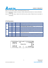
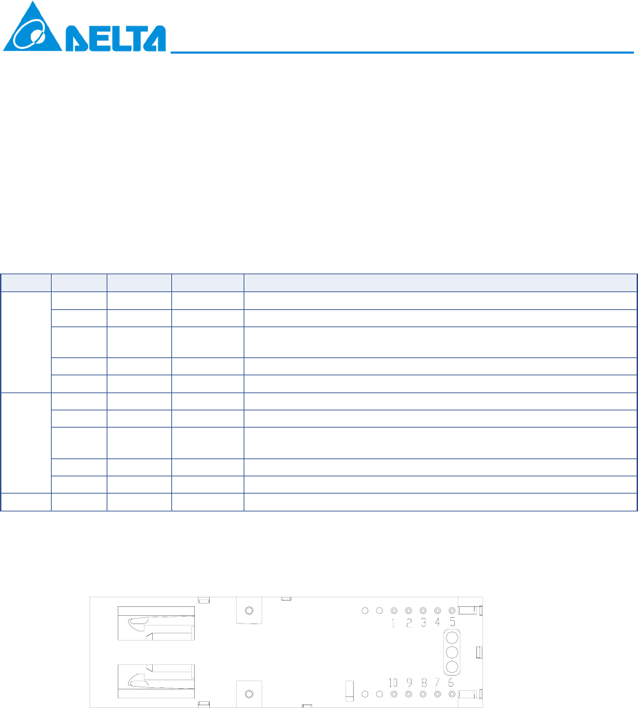
6. Pin Description
Tx/Rx Pin No. I/O Pin Name Description
1
VeeR
Receiver Ground
2
VccR
+3.3V Receiver Power Supply
3 O
SD Normal Optical Input indicated by logic “High”, and No Optical
Input indicated by logic “Low”. (LVTTL)
4 O
RD(n)
Inverted Receiver Data Output (AC-Coupled CML output)
Rx
5 O
RD(p)
Non-Inverted Receiver Data Output (AC-Coupled CML output)
6
VccT
+3.3V Transmitter Power Supply
7
VeeT
Transmitter Ground
8 I
Tx_Dis LVTTL Logic “High” to Disable Transmitter, and Enable
Transmitter by Logic “Low”.
9 I
TD(p)
Non-Inverted Transmitter Data Input (AC-Coupled LVPECL input)
Tx
10 I
TD(n)
Inverted Transmitter Data Input (AC-Coupled LVPECL input)
MS
Mounting studs/ connect this pin to Chassis ground
Note (1). EMI shielding lead must be connected to Signal ground
Bottom View
MS
MS