Design Guide & Applications Manual
For VI-200 and VI-J00 Family DC-DC Converters and Configurable Power Supplies
vicorpower.com 800-735-6200 Applications Engineering 1-800-927-9474 Rev. 2.1
Page 23 of 88
9. EMC Considerations
RADIATED NOISE
Radiated noise may be either electric field or magnetic
field. Magnetic radiation is caused by high di/dt and is
generally what is measured by FCC, VDE or MIL-STD-461.
Vicor converters utilize zero-current-switching, with the
advantage over PWM non-zero-current-switching being
that zero-current-switching topologies contain minimal
discontinuities in the switched current waveforms,
resulting in lower di/dt’s. Electric field radiation (caused by
dv/dt) is “near-field,” i.e., it decays rapidly as a function of
distance and as a result does not typically affect radiated
measurements.
Radiation can be minimized by proper board layout. Keep
all leads with AC current short, twisted or routed as
overlapping planes to minimize loop cross-sectional area.
Also keep in mind the effects of capacitive coupling —
even when not expected. Do not put an unshielded filter
on the opposite side of the PCB from the module.
Conducted noise can be capacitively coupled around the
filter. Do not route input and output leads in the same
cable bundle. Again, no special precautions, just good
design practice.
NOISE CONSIDERATIONS
All switchmode power supplies generate a certain amount
of “noise”, yet it remains one of the least understood
parameters in power conversion.
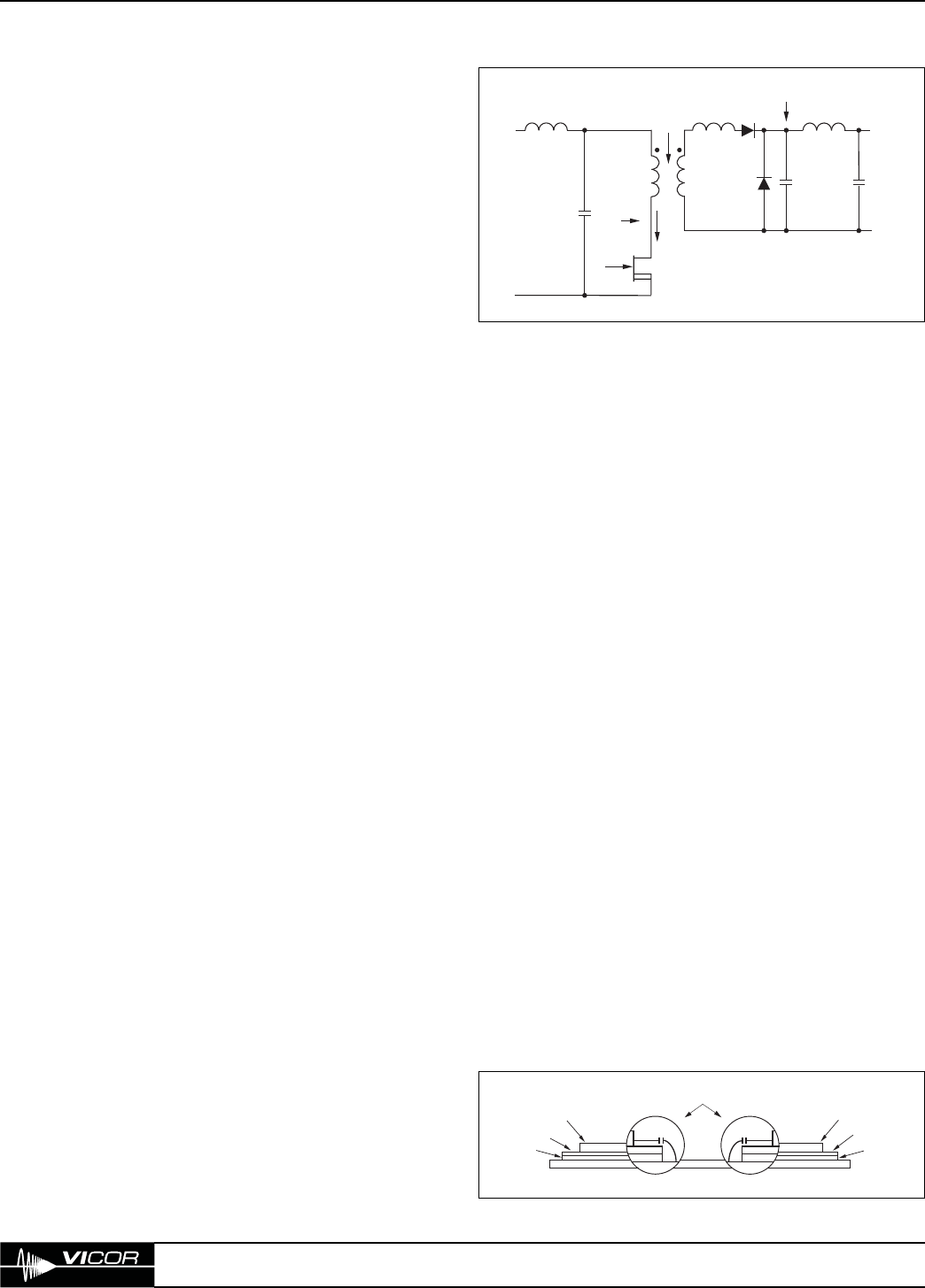
VI-200s and VI-J00s both use the same topology, so their
operation is very similar. These products are zero-current-
switching converters — i.e., the current is zero when the
main switch is turned on or off. While the switch is on,
the current through the switch or the primary of the
transformer is a half-wave rectified sine wave. Similar in
operation to a resonant converter, these products are
commonly referred to as quasi-resonant converters. The
LC resonant frequency is fixed so the on-time of the
switch is about 500 ns. When the switch turns on, energy
builds up in the leakage inductance of the transformer (L)
and then “transferred” into the capacitor on the
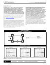
secondary side of the module. (C, Figure 9–6) The energy
processed in each pulse is fixed, and is ultimately the
energy stored in this capacitor, 1/2 CV
2
. Since the energy
in every pulse is fixed, the repetition rate of the pulse train
is varied as a function of load to regulate the output
voltage. Maximum repetition rate occurs at minimum line,
full load and is approximately twice the LC time period or
1 µs. If the load drops by 50%, then the repetition rate is
approximately one-half of maximum (since the energy in
every pulse is fixed). Therefore the pulse repetition rate
varies linearly with load, to a first order approximation.
Since the energy in every pulse is related to the square of
the applied voltage (CV
2
), the pulse repetition rate varies
as approximately the square of the line voltage. For
example, a 300 V input unit can vary from 200 – 400 V,
or a factor of two, therefore it follows that the repetition
rate must vary by approximately a factor of four to regulate
the output. As previously established, the current in the
primary is a half-wave rectified sine wave, but the voltage
on the primary is a square wave. Since this voltage is a
square wave, it contains harmonics of the fundamental
switching frequency. It also includes frequencies, that extend
to 70 MHz.
These frequencies can be of interest in the following
circumstances. Rapidly changing voltages (high dv/dt) can
generate E-fields (primarily near-field) which do not usually
cause system noise problems since they significantly
decrease as a function of distance. For this reason, E-fields
are not measured by agencies such as the FCC or VDE.
These agencies do, however, measure the magnetic
radiation caused by high frequency currents in a conductor.
The half-wave rectified sine wave in the transformer is an
example of this, but since there are minimal discontinuities
in the current waveform and the loop cross-sectional area
is very small, the resultant E-field is very small. E-fields can
be a problem if sensitive circuitry is located near the
module. In this case, a shield can be positioned under the
label side of the module as a discrete element or as a
ground plane on the PCB. The other effect that occurs as
a result of the 50 – 70 MHz component on the main
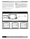
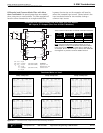
switch is common-mode noise. (Figure 9–7)
L
C
Vs
Ip
+IN
–IN
Vp
+ OUT
–OUT
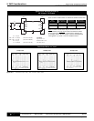
Figure 9–6 — Basic zero-current-switching converter topology
(VI-200 / VI-J00)
Ceramic
Parasitic
Capacitance
Baseplate
Rectifier
Ceramic
FET
ShieldShield
Figure 9–7 — The shield layer serves to reduce the capacitance


