ETX-945 User Manual 1.00 www.diamondsystems.com Page 17
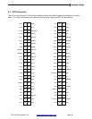
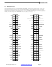
4.1.1 PCI bus signals
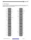
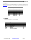
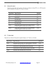
This set of pins implements the module’s PCI expansion bus. For further information regarding the functions of
the PCI bus signals, refer to the PCI Bus Specification, available from the PCI Special Interest Group
(http://www.pcisig.com/specifications).
Signal Name
Signal function
Direction
PCICLK1-4
PCI clock outputs for external PCI devices
Out
REQ0-3#
Bus Request signals of PCI Masters
In
GNT0-3#
Grant signals to PCI Masters
Out
AD0-31
PCI address and data bus signals
In/Out
CBE0-3#
PCI Bus command and byte enables
In/Out
PAR
PCI bus parity bit
In
SERR#
System Error or PCI Clock RUN
In/Out
GPERR#
Parity Error
In/Out
PME#
Power management event
In/Out
LOCK#
Lock resource signal
In/Out
DEVSEL#
Device select
In/Out
TRDY#
Target ready
In/Out
IRDY#
Initiator ready
In/Out
STOP#
Stop
In/Out
FRAME#
Cycle frame
In/Out
PCIRST#
PCI bus reset
Out
INTA#
PCI interrupt A
In
INTB#
PCI interrupt B
In
INTC#
PCI interrupt C
In
INTD#
PCI interrupt D
In


