


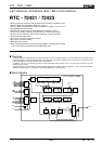
RTC - 72421 / 72423
Page - 7 MQ - 162 - 03
Registers
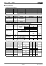
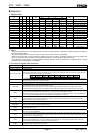
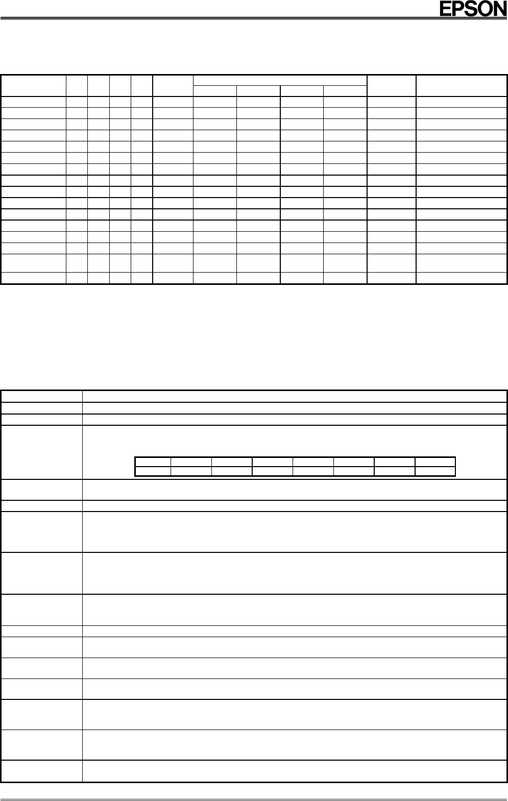
1. Register table
Data
Address
(Hex)
A3 A2 A1 A0
Register
name
D3 D2 D1 D0
Count
(BCD)
Remarks
0 0 0 0 0 S1 s8 s4 s2 s1 0 to 9 1-second di
g
it re
g
ister
1 0 0 0 1 S10 * s40 s20 s10 0 to 5 10-seconds digit register
2 0 0 1 0 MI1 mi8 mi4 mi2 mi1 0 to 9 1-minute digit register
3 0 0 1 1 MI10 * mi40 mi20 mi10 0 to 5 10-minute digit register
4 0 1 0 0 H1 h8 h4 h2 h1 0 to 9 1-hour digit register
5 0 1 0 1 H10 * PM/AM h20 h10 0 to1 or 2 10-hours digit register
6 0 1 1 0 D1 d8 d4 d2 d1 0 to 9 1-day digit register
7 0 1 1 1 D10 * * d20 d10 0 to 3 10-days digit register
8 1 0 0 0 MO1 mo8 mo4 mo2 mo1 0 to 9 1-month digit register
9 1 0 0 1 MO10 * * * mo10 0 to 1 10-months digit register
A 1 0 1 0 Y1 y8 y4 y2 y1 0 to 9 1-year digit register
B 1 0 1 1 Y10 y80 y40 y20 y10 0 to 9 10-years digit register
C 1 1 0 0 W * w4 w2 w1 0 to 6 Day-of-the-week register
D 1 1 0 1 CD 30s ADJ IRQ FLAG BUSY HOLD Control register D
E 1 1 1 0 CE t1 t0
ITRPT/
STND
MASK Control register E
F 1 1 1 1 CF TEST 24/12 STOP RESET Control register F
2. Notes
The counts at addresses 0 to C are all positive logic. Therefore, a register bit that is 1 appears as a high-level signal on the data bus.
Data representation is BCD.
Do not set an impossible date or time in the RTC. If such a value is set, the effect is unpredictable.
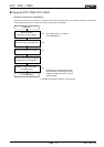
When the power is turned on (before the RTC is initialized), the state of all bits is undefined. Therefore, write to all registers after
power-on, to set initial values. For details of the initialization procedure, see "Using the RTC-72421/RTC-72423".
The TEST bit of control register F is used by EPSON for testing. Operation cannot be guaranteed if 1 is written to this bit, so make
sure that it is set to 0 during power-on initialization.
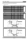
3. Functions of register bits (overview)
Bit name Function
* mark Not used. Writing to this bit has no effect; reading it always returns 0.
Seconds to year digit All written BCD code.
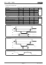
Day-of-the-week digit
This is special (base 7) counter that increments each time the day digits are incremented. It counts from 0 to 6. Since the value in the
counter bears no relationship to the day of the week, the user can choose the coding that relates the counter value to the day of the
week. The following is just one example of this relationship.
Count 0 1 2 3 4 5 6
Day Sunday Monday Tuesday Wednesday Thursday Friday Saturday
PM/AM
The PM/AM bit is 1 for p.m. times; 0 for a.m. times. This bit is valid only for 12-hour-clock mode (when the 24/12 bit is 0); in 24-hour-
clock mode (when the 24/12 bit is 1), this bit is always 0.
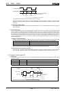
30-seconds ADJ Writing 1 to this bit executes a 30-seconds correction.
IRQ FLAG
The IRQ FLAG bit is set to 1 when an interrupt request is generated in fixed-period interrupt mode. Writing 0 to this bit clears it. Note
that it is possible to write 1 to this bit, but this will have no effect.
In fixed-period pulse output mode, this bit is at 1 while the pulse output is active(While the STD.P pin output is low), and is
automatically cleared when pulse output ends. Writing 0 to this bit while pulse output is active forcibly cancels the pulse output.
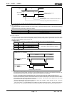
BUSY
Use the BUSY bit when accessing data in the S
1
to W registers. This bit is set to 1 during the incrementation cycle of the S
1
to W
registers, and is set to 0 otherwise. When the BUSY bit is 1, access to the S
1
to W registers is inhibited.
Note that the HOLD bit must also be used when accessing the S
1
to W registers. The BUSY bit is always 1 when the HOLD bit is 0.
There is no need to check the BUSY bit when accessing the control registers (C
D
, C
E
and C
F
).
HOLD
When 1 has been written to the HOLD bit, the status of the BUSY bit can be checked. While the HOLD bit is 1, any incrementation of
the digits is held just once. (The incrementation is held only once, even if the HOLD bit remains at 1 for two or more seconds.)
Clear the HOLD bit to 0 by forcing the CS1 pin low.
t1,t0 These bits set the timing for fixed-period pulse output and interrupts (1/64 seconds, 1 second, 1minute or 1 hour).
ITRPT/STND
The ITRPT/STND bit sets fixed-period pulse output mode and fixed-period interrupt mode. Write 1 to this bit to set interrupt(INRPT)
mode; when write 0 to it to set pulse output(STND) mode.
MASK
The MASK bit disables fixed-period pulse output and fixed-period interrupts. Write 1 to this bit to mask and inhibit these modes; write
0 to it to enable these modes.
TEST
The TEST bit is used by EPSON for test purposes. Operation cannot be guaranteed if 1 is written to this bit, so make sure that it is
set to 0 during power-on initialization.
24/12
The 24/12 bit switches between 24-hour clock and 12-hour clock. Write 1 to this bit to set 24-hour mode; write 0 to it to set 12-hour
mode. When the 24/12 bit is set, both the timer registers and the timer mode must be reset to match. Note that the h20 bit of the H10
register is always in 12-hour-clock mode.
STOP
The STOP bit sets an inhibition on clock operation in 8192 Hz steps which are divisions of the 1 second signal from the RTC’s
internal 32768 Hz oscillation source. The clock is inhibited when the STOP bit is 1, and released again when it becomes 0. The
internal oscillation circuit continues to operate even when the STOP bit is 1.
RESET
The RESET bit resets the part of the counter that is below one second. Write 1 to this bit to reset; 0 to release the reset.
The RESET bit set to 0 when the CS1 pin goes low.