


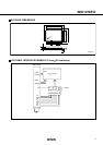
SED1278F/D
2
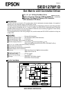
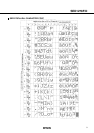
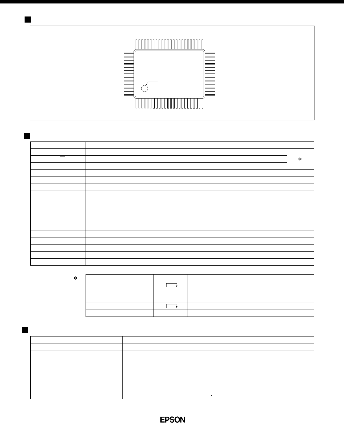
PIN CONFIGURATION
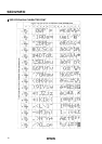
PIN DESCRIPTION
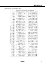
ABSOLUTE MAXIMUM RATINGS
INDEX
1
510152025
30
35
404550556065
80
75
70
SED1278F
SEG38
SEG37
SEG36
SEG35
SEG34
SEG33
SEG32
SEG31
SEG30
SEG29
SEG28
SEG27
SEG26
SEG25
SEG24
SEG23
DB1
DB0
E
R/W
RS
D0
FR
V
DD
XSCL
LP
V5
V4
V3
V2
V1
OSC2
SEG39
SEG40
COM16
COM15
COM14
COM13
COM12
COM11
COM10
COM9
COM8
COM7
COM6
COM5
COM4
COM3
COM2
COM1
DB7
DB6
DB5
DB4
DB3
DB2
SEG22
SEG21
SEG20
SEG19
SEG18
SEG17
SEG16
SEG15
SEG14
SEG13
SEG12
SEG11
SEG10
SEG9
SEG8
SEG7
SEG6
SEG5
SEG4
SEG3
SEG2
SEG1
V
SS
OSC1
QFP5-80pin
Unit: mm
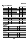
Rating
Supply voltage (1)
Supply voltage (2)
Input voltage
Output voltage
Power dissipation
Operating temperature
Storage temperature
Soldering temperature and time
Symbol
V
DD
V
1
to V
5
V
I
V
O
P
D
T
opr
T
stg
T
sol
Unit
V
V
V
V
mW
˚C
˚C
—
Value
-0.3 to 7.0
-0.3 to V
DD
+0.3
-0.3 to V
DD
+0.3
-0.3 to V
DD
+0.3
300
-20 to 75
-65 to 150
260˚C 10s (at lead)
(V
SS
=0V, Ta=25˚C)
Symbol
RS
R/W
E
DB0 to DB7
LP
XSCL
FR
DO
COM 1 to COM16
SEG1 to SEG40
V1 to V5
V
DD
V
SS
OSC1
OSC2
No. of signals
1
1
1
8
1
1
1
1
16
40
5
1
1
2
0
0
1
1
1
1
Function
Register select signal
Read/write select signal
Read/write execute signal
Data bus
Data latching pulse
Data transfer clock
LCD AC driving signal
Serial data
Common outputs
COM9 to COM16: non-select for 1/8 duty
COM12 to COM16: non-select for 1/11 duty
Segment outputs
LCD driving power (V
5
>
=
V
SS
)
+5V
0V (GND)
Used to connect resistor (typ. 91K-ohms) for oscillation;
OSC1 is for external clock input.
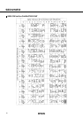
Instruction write cycle
DD RAM or CG RAM data write cycle
DD RAM or CG RAM data read cycle
Busy flag read cycle
Address counter read cycle
RS
0
11
1
0
1
R/W E Operation
Note: The following condition must always hold true: V
DD
>
=
V
1
>
=
V
2
>
=
V
3
>
=
V
4
>
=
V
5