


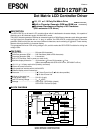
3
SED1278F/D
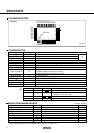
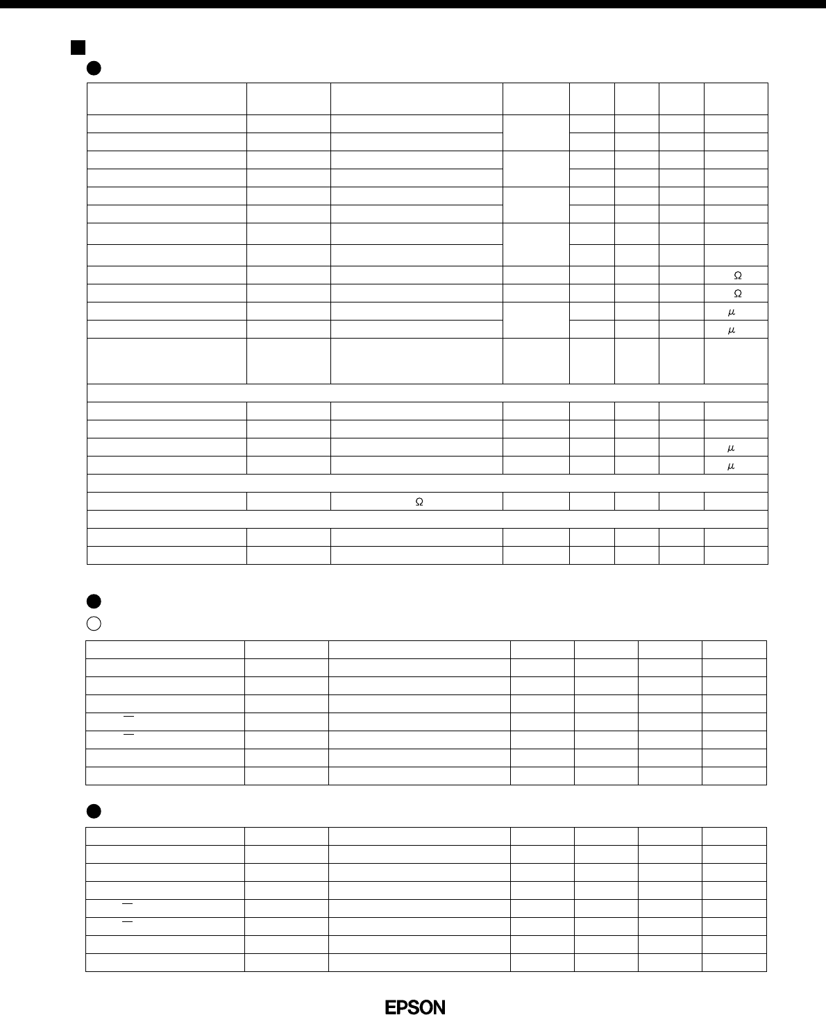
ELECTRICAL CHARACTERISTICS
DC Characteristics
Write Cycle
V
IH1
V
IL1
V
IH2
V
IL2
V
OH1
V
OL1
V
OH2
V
OL2
R
COM
R
SEG
I
IL
-I
P
I
OP
f
EXTCL
Duty
tr
EXTCL
tf
EXTCL
f
OSC
f
OSC
V
LCD
Symbol
I
OH
=-0.205mA
I
OL
=1.6mA
I
OH
=-0.04mA
I
OL
=0.04mA
|V
COM
-V
n
|=0.5V
|V
SEG
-V
n
|=0.5V
V
I
=0 to V
DD
V
DD
=5V
R
f
=91K ±2%
Ceramic filter
V
DD
-V
5
Condition
2.0
V
SS
V
DD
-1.0
V
SS
2.4
—
0.9V
DD
—
—
—
—
50
—
125
45
-
-
190
245
3.0
Min.
DB0~DB7
RS, R/W, E
OSC1
DB0~DB7
V
DD
COM1~16
SEG1~40
Applicable
Pin
—
—
—
—
—
—
—
—
2
2.5
—
125
250
50
—
—
270
250
—
0.5
Typ.
V
DD
0.8
V
DD
1.0
—
0.4
—
0.1V
DD
10
10
1
250
350
55
0.2
0.2
350
255
V
DD
0.8
Max.
V
V
V
V
V
V
V
V
k
k
A
A
mA
kHz
%
S
S
kHz
kHz
V
Unit
"H" level input voltage (1)
"L" level input voltage (1)
"H" level input voltage (2)
"L" level input voltage (2)
"H" level output voltage (1)
"L" level output voltage (1)
"H" level output voltage (2)
"L" level output voltage (2)
Driver-on resistor (COM)
Driver-on resistor (SEG)
I/O leakage current
Pull-up MOS current
Supply current
External clock operation
External clock operating frequency
External clock duty
External clock rise time
External clock fall time
Internal clock operation (Rf oscillation)
Oscillation frequency
Internal clock operation (Ceramic filter oscillation)
Oscillation frequency
LCD driving voltage
Characteristic
Rf oscillation, from
external clock
V
DD
=5V, fosc=f
CP
=270kHz
(V
DD
=5.0V±10%, V
SS
=0V, Ta=-20 to 75˚C)
XSCL
LP
DO
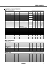
AC Characteristics
Read Cycle
t
cycE
t
WEH
t
rE
, t
fE
t
AS
t
AH
t
RD
t
DHR
Symbol
500
220
—
40
10
—
20
Min.
—
—
—
—
—
—
—
Typ.
—
—
25
—
—
120
—
Max.
ns
ns
ns
ns
ns
ns
ns
Unit
C
L
=100pF
Condition
Enable cycle time
Enable "H" level pulse width
Enable rise/fall time
RS, R/W setup time
RS, R/W address hold time
Read data output delay
Read data hold time
Characteristic
(V
DD
=5.0V±10%, V
SS
=0V, Ta=-20 to 75˚C)
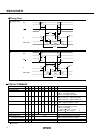
t
cycE
t
WEH
t
rE
, t
fE
t
AS
t
AH
t
DS
t
DH
Symbol
500
220
—
40
10
60
10
Min.
—
—
—
—
—
—
—
Typ.
—
—
25
—
—
—
—
Max.
ns
ns
ns
ns
ns
ns
ns
UnitCondition
Enable cycle time
Enable "H" level pulse width
Enable rise/fall time
RS, R/W setup time
RS, R/W address hold time
Data setup time
Write data hold time
Characteristic
(V
DD
=5.0V±10%, V
SS
=0V, Ta=-20 to 75˚C)