


©2002 Fairchild Semiconductor Corporation Application Note 7502 Rev. A1
For peak gate voltages other than 10 volts, and load resis-
tances other than BV
DSS
/I
D(MAX)
, the equations of Table 1
may be used in conjunction with slope estimates from the
characterization curves for C
X
and C
GS
+ C
X
(1 + g
M
/g
MJ
) at
the appropriate drain-current level.
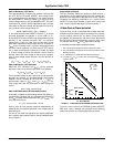
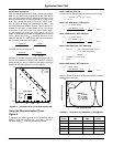
Characterization-Curve Limits
The switching-time range over which the characterization can be
applied is very impressive. For gate currents of the order of
microamperes, device dissipation is the limiting factor. For gate
currents of the order of amperes, the device response will be
slowed by gate propagation delay. This delay, of course,
degrades the linear switching relationship to gate current. How-
ever, as Figure 12 graphically shows, the characterization is valid
across five decades of gate current and switching time, allowing
all but a very few switching applications to be described by the
characterization curves of Figure 9.
FIGURE 12. FIVE DECADES OF LINEAR RESPONSE
Conclusions
The viability of the proposed characterization curves using con-
stant current has been demonstrated and the limits of applica-
tion defined. The existence of a vertical JFET in a power
MOSFET makes data-sheet capacitances of little use for esti-
mating switching times. The classical method of defining
switching time by 10% and 90% is a poor representation for
power MOSFETs because of the dual-slope nature of the drain
waveforms. Switching influences are masked because the 10%
level is controlled by one mechanism and the 90% level by
another. Device comparisons based on the classical switching
definition can be very misleading.
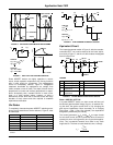
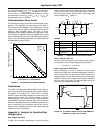
Appendix A - Analysis for Resistive Step
Voltage Inputs
Step Voltage Gate Drive
To obtain the necessary relationships, six device switching
states must be examined using the same device equivalent
circuit as was used for the constant-gate-current case, but
with the forcing function replaced wIth a step voltage with
internal resistance R
O
, Figure A-1.
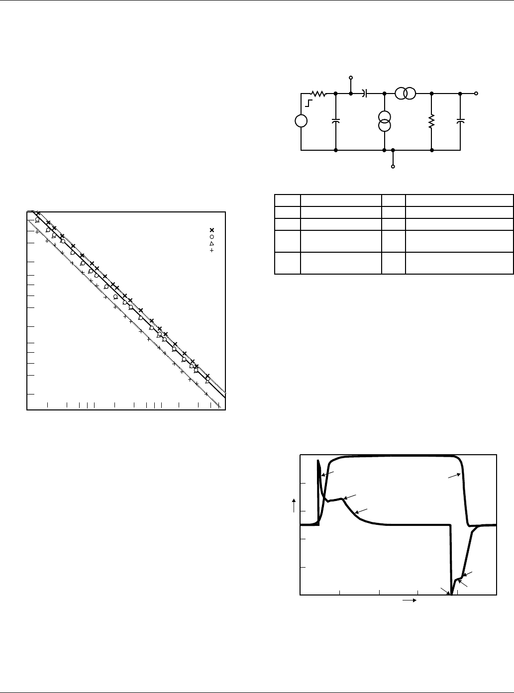
FIGURE A-1. POWER MOSFET EQUIVALENT CIRCUIT
State 1: Mos Off, JFET Off
As before, both current generators are open circuits, reducing
the equivalent circuit to simply charging C
ISS
through R
O
.
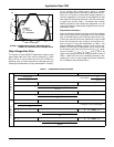
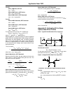
State 2: Mos Active, JFET Active
Before proceeding, it is wise to examine an actual device
response and make use of available simplifications. Figure A-2
shows i
G
(t) and i
D
(t) for a typical power MOSFET driven by a
step gate voltage. For truly resistive switching, realize that these
waveforms are only mirror images of their voltage counterparts
v
G
(t) and v
D
(t). Using Figure A-2, applicable gate currents for
each of the device states may be listed.
FIGURE A-2. i
G
(t) AND i
D
(t) FOR A TYPICAL POWER MOSFET
DRIVEN BY A STEP GATE VOLTAGE
10
4
10
2
10
0
10
-2
10
0
10
2
10
4
RFM15N15
t
D
(OFF)
t
R
t
F
t
D
(ON)
GATE CURRENT (I
G
) - MICROAMPERES
TIME(t) - MICROSECONDS
10
3
10
1
10
-1
10
1
10
3
10
5
10
6
LEGEND
V
GS
- Gate Voltage C
DS
- Drain Source Capacitance
V
X
- JFET Driving Voltage g
M
- MOSFET Transconductance
V
D
- Drain Voltage g
MJ
- JFET Transconductance
C
GS
- Gate Source
Capacitance
R
L
- Drain Load Resistance
C
X
- MOSFET Feedback
Capacitance
I
G
- Constant Current Amplitude
t = R
O
C
ISS
In(1/(1 - V
GS(TH)
/V
G
)]
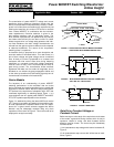
GATE
C
DS
SOURCE
DRAIN
C
X
V
GS
V
G
g
MJ
V
X
R
L
C
GS
g
M
V
G
V
D
V
X
R
O
I
PK1
I
PK2
I
PK3
I
PK4
I
PK5
I
PK6
CURRENT
TIME
i
D
(t)
i
G
(t)
Application Note 7502