© 2009 Fairchild Semiconductor Corporation www.fairchildsemi.com
FPF2300/02/03 • Rev. 1.1.3 15
FPF2300/02/03 — Dual-Output Current Limit Switch
PCB Layout Recommendations
For the best performance, all traces should be as short as
possible. To be most effective, the input and output capacitors
should be placed close to the device to minimize the effects that
parasitic trace inductances may have on normal and short-
circuit operation. Using wide traces for IN, OUTs, and GND pins
helps minimize parasitic electrical effects and the case-to-
ambient thermal impedance.
Improving Thermal Performance
Improper layout could result in higher junction temperature and
triggering the thermal shutdown protection feature. This concern
is particularly significant for the FPF2303, where both channels
operate in constant current mode in the overload conditions and
during fault condition the outputs are shorted, resulting in large
voltage drop across switches. In this case, power dissipation of
the switch (P
D
= (V
IN
- V
OUT
) x I
LIM(MAX)
) could exceed the
maximum absolute power dissipation of part.
The following techniques improve the thermal performance of
this family of devices. These techniques are listed in order of
the significance of impact.
1. Thermal performance of the load switch can be improved
by connecting the DAP (Die Attach Pad) of MLP 3x3mm
package to the GND plane of the PCB.
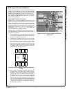
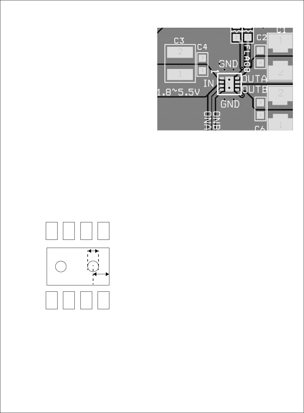
2. Embedding two exposed through-hole vias into the DAP
(pin 9) provides a path for heat to transfer to the back GND
plane of the PCB. A drill size of round, 15 mils (0.4mm),
with 1-ounce copper plating is recommended to create
appropriate solder reflow. A smaller size hole prevents the
solder from penetrating into the via, resulting in device lift-
up. Similarly, a larger via hole consumes excessive solder
and may result in voiding of the DAP.
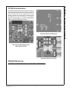
Figure 41. Two Through-Hole Open Vias Embedded
in DAP
3. The IN, OUTs, and GND pins dissipate most of the heat
generated during a high load current condition. Figure 42
illustrates a proper layout for devices in MLP 3x3mm
packages. IN, OUTs, and GND pins are connected to
adequate copper so heat may be transferred as efficiently
as possible out of the device. The low-power FLAGB and
ON pin traces may be laid out diagonally from the device to
maximize the area available to the ground pad. Placing the
input and output capacitors as close to the device as
possible also contributes to heat dissipation, particularly
during high load currents.
Figure 42. Proper Layout of Output and Ground
Copper Area
15mil
25mil


