© 2009 Fairchild Semiconductor Corporation www.fairchildsemi.com
FPF2300/02/03 • Rev. 1.1.3 12
FPF2300/02/03 — Dual-Output Current Limit Switch
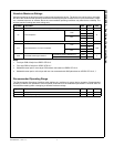
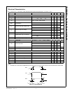
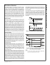
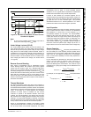
Figure 37. FPF2300 FLAGB While and Over-Current
Condition is Applied
Note:
7. An over-current condition signal loads the output with a
heavy load current larger than I
LIMIT
value.
Under-Voltage Lockout (UVLO)
The under-voltage lockout feature turns off the switch if the
input voltage drops below the under-voltage lockout threshold.
With the ON pin active (ON pin pulled LOW), the input voltage
rising above the under-voltage lockout threshold causes a
controlled turn-on of the switch and limits current overshoot. If a
device is in UVLO condition, both FLAGBs go LOW and indicate
the fault condition. The device detects the UVLO condition when
input voltage goes below UVLO voltage, but remains above
1.3V (typical).
Reverse Current Blocking
Each switch of FPF2300/2/3 has an independent reverse
current blocking feature that protects input source against
current flow from output to input. For a standard USB power
design, this is an important feature that protects the USB host
from being damaged due to reverse current flow on V
BUS
. To
activate the reverse current blocking, the switch must be in OFF
state (ON pins inactivated) so that no current flows from the
output to the input. The FLAGB operation is independent of the
reverse current blocking and does not report a fault condition if
this feature is activated.
Thermal Shutdown
The thermal shutdown protects the device from internally or
externally generated excessive temperatures. Each switch has
an individual thermal shutdown protection function and operates
independently as adjacent switch temperatures increase above
140°C. If one switch is in normal operation and shutdown
protection of second switch is activated, the first channel
continues to operate if the affected channel's heat stays
confined. The over-temperature in one channel can shut down
both switches due to rapidly generated excessive load currents
resulting in very high power dissipation. Generally, a thermally
improved board layout can provide heat sinking and allow heat
to stay confined and not affect the second switch operation.
During an over-temperature condition, the FLAGB is pulled
LOW and the affected switch is turned off. If the temperature of
the die drops below the threshold temperature, the switch
automatically turns on again. To avoid unwanted thermal
oscillations, a 10°C (typical) thermal hysteresis is implemented
between thermal shutdown entry and exit temperatures.
If output of both switches are connected together and an
excessive load current activates thermal protection of both, the
controller can shut down the switches after both FLAGB outputs
go LOW and turn on both channels again. This provides
simultaneous switch turn on. Thermal protection is for device
protection and should not be used as regular operation.
Input Capacitor
To limit the voltage drop on the input supply caused by transient
inrush currents when the switch is turned on into discharged
load capacitors or a short-circuit; an input capacitor, C
IN
, is
recommended between IN and GND. The FPF2310/2/3/3L
features a fast current limit response time of 20μs. An inrush
current (also known as surge current) could occur during the
current limit response time while the switch is responding to an
over-current condition caused by large output capacitors. A
10μF ceramic capacitor, C
IN
, is required to provide charges for
the inrush current and prevent input voltage drop at turn on.
Higher values of C
IN
can be used to further reduce voltage drop.
Output Capacitor
A 0.1μF to 1μF capacitor, C
OUT
, should be placed between the
OUT and GND pins. This capacitor prevents parasitic board
inductances from forcing output voltage below GND when the
switch turns off. This capacitor should have a low dissipation
factor. An X7R MLCC (Multilayer Ceramic Chip) capacitors is
recommended.
For the FPF2300 and FPF2302, the total output capacitance
needs to be kept below a maximum value, C
OUT(MAX)
, to
prevent the part from registering an over-current condition
beyond the blanking time and shutdown. The maximum output
capacitance for a giving input voltage can be determined from
the following:
For example, in a 5V application, C
OUT(MAX)
can be determined
as:
VIN
ON
FLAGB
VOUT
Startup
tBLANK
ILOAD
ILIMIT
Over
current
condtion
Thermal Shutdown
Device Cools Off
(1)
C
OUT(MAX)
=
I
LIM(MIN)
x t
BLANK(MIN)
V
IN
(2)
C
OUT(MAX)(IN = 5V)
=
1.1A x 5ms
5
=
1.1mF


