


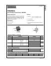
FDD6690A Rev. EW)
D
R
P
DS(ON)
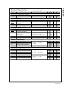
Electrical Characteristics T
A
= 25°C unless otherwise noted
Symbol Parameter Test Conditions Min Typ Max Units
Drain–Source Diode Characteristics and Maximum Ratings
I
S
Maximum Continuous Drain–Source Diode Forward Current 2.3 A
V
SD
Drain–Source Diode Forward Voltage
V
GS
= 0 V, I
S
= 2.3 A (Note 2)
0.76 1.2 V
t
rr
Diode Reverse Recovery Time 24 nS
Q
rr
Diode Reverse Recovery Charge
I
F
= 12 A, d
iF
/d
t
= 100 A/µs
13 nC
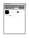
Notes:
1. R
θJA
is the sum of the junction-to-case and case-to-ambient thermal resistance where the case thermal reference is defined as the solder mounting surface of
the drain pins. R
θJC
is guaranteed by design while R
θCA
is determined by the user's board design.
a) R
θJA
= 45°C/W when mounted on a
1in
2
pad of 2 oz copper
b) R
θJA
= 96°C/W when mounted
on a minimum pad.
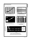
Scale 1 : 1 on letter size paper
2. Pulse Test: Pulse Width < 300µs, Duty Cycle < 2.0%
3. Maximum current is calculated as:
where P
D
is maximum power dissipation at T
C
= 25°C and R
DS(on)
is at T
J(max)
and V
GS
= 10V. Package current limitation is 21A
FDD6690A