


3 www.fairchildsemi.com
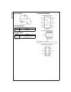
NC7SB3257
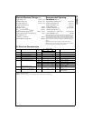
Absolute Maximum Ratings(Note 1) Recommended Operating
Conditions
(Note 2)
Note 1: Absolute maximum ratings are DC values beyond which the device
may be damaged or have its useful life impaired. The datasheet specifica-
tions should be met, without exception, to ensure that the system design is
reliable over its power supply, temperature, and output/input loading vari-
ables. Fairchild does not recommend operation outside datasheet specifi-
cations.
Note 2: Control input must be held HIGH or LOW, it must not float.
Note 3: The input and output negative voltage ratings may be exceeded if
the input and output diode current ratings are observed.
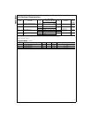
DC Electrical Characteristics
Note 4: Measured by the voltage drop between A and B pins at the indicated current through the switch. On Resistance is determined by the lower of the
voltages on the two (A or B Ports).
Note 5: Per TTL driven Input (V
IN
= 3.4V, Control input only). A and B pins do not contribute to I
CC
.
Supply Voltage (V
CC
) −0.5V to +7.0V
DC Switch Voltage (V
S
) −0.5V to +7.0V
DC Output Voltage (V
IN
) −0.5V to +7.0V
DC Input Diode Current (I
IK
)
@ (I
IK
) V
IN
< 0V −50 mA
DC Output Current (I
OUT
) 128 mA
DC V
CC
or Ground Current (I
CC
/I
GND
) ±100 mA
Storage Temperature Range (T
STG
) −65°C to +150°C
Junction Lead Temperature under Bias (T
J
) +150°C
Lead Temperature (T
L
)
(Soldering, 10 seconds)
+260°C
Power Dissipation (P
D
) @ +85°C180 mW
Supply Voltage Operating (V
CC
) 4.0V to 5.5V
Control Input Voltage (V
IN
)0V to V
CC
Switch Input Voltage (V
IN
)0V to V
CC
Output Voltage (V
OUT
)0V to V
CC
Operating Temperature (T
A
) −40°C to +85°C
Input Rise and Fall Time (t
r
, t
f
)
Control Input V
CC
= 4.0V to 5.5V 0 ns/V to 5 ns/V
Thermal Resistance (
θ
JA
)350°C/W
Symbol Parameter
V
CC
T
A
= −40°C to +85°C
Units Conditions
(V) Min Typ Max
V
IK
Clamp Diode Voltage 4.5 −1.2 V I
IN
= −18 mA
V
IH
HIGH Level Input Voltage 4.5 − 5.5 2.0 V
V
IL
LOW Level Input Voltage 4.5 − 5.5 0.8
I
IN
Input Leakage Current 5.5 ±1 µA0 ≤ V
IN
≤ 5.5V
I
OFF
OFF State Leakage Current 5.5 ±1 µA0 ≤ A, B ≤ V
CC
R
ON
Switch ON Resistance (Note 4) 4.5 3 7 Ω V
IN
= 0V, I
IN
= 64 mA
4.5 3 7 Ω V
IN
= 0V, I
IN
= 30 mA
4.5 6 15 Ω V
IN
= 2.4V, I
IN
= 15 mA
4.0 10 20 Ω V
IN
= 2.4V, I
IN
= 15 mA
I
CC
Quiescent Supply Current 5.5 10 µAV
IN
= V
CC
or GND
I
OUT
= 0
∆I
CC
Increase in I
CC
Per Input (Note 5) 5.5 0.9 2.5 mA V
IN
= 3.4V, I
O
= 0
Control Input Only