MB3788
5
■
■■
■
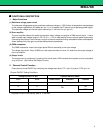
FUNCTIONAL DESCRIPTION
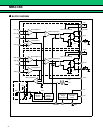
1. Major Functions
(1) Reference voltage power circuit
The reference voltage power supply produces a reference voltage (≈ 2.50 V) which is temperature-compensated
by the voltage supplied from the power pin (pin 11); it is used as the IC internal circuit operating power supply.
The reference voltage can also be output externally at 1 mA from V
REF
pin (pin12).
(2) Error amplifier
The error amplifier detects the switching regulator output voltage and outputs a PWM control signal. It has a
wide in-phase input voltage range of -0.2 V to V
CC
- 1.8 V to make setting from an external power supply easy.
Connecting the output pin and inversion input pin of the error amplifier through a feedback resistor and capacitor
allows setting of any loop gain to provide stable phase compensation.
(3) PWM comparator
The PWM comparator controls the output pulse ON time according to the input voltage.
The voltage input to the -IN pin (PWM) turns the output transistor on when it is lower than the output voltage of
the error amplifier.
(4) Output circuit
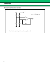
The output circuit is configured in a push-pull form and uses a PNP transistor drive system to drive a transistor
of up to 30 mA. (See
How to Set Output Current.
)
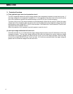
2. Channel Control Function
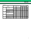
Channels can be set ON/OFF by combining the voltage levels at pin CTL1 (pin 13) and pin CTL2 (pin 14).
Channel ON/OFF Setting Conditions
*: The power current in the standby state is 10 µA Max.
Voltage level at CTL pin Channel ON/OFF status
CTL1 CTL2 Power circuit Channel 1 Channel
L × Stand by state*
HH
ON
ON
LOFF


