MB3887
4
■
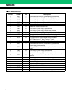
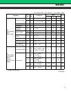
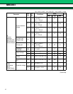
PIN DESCRIPTION
Pin No. Symbol I/O Descriptions
1 −INC2 I Current detection amplifier (Current Amp2) input terminal.
2 OUTC2 O Current detection amplifier (Current Amp2) output terminal.
3 +INE2 I Error amplifier (Error Amp2) non-inverted input terminal.
4 −INE2 I Error amplifier (Error Amp2) inverted input terminal.
5 FB2 O Error amplifier (Error Amp2) output terminal.
6 VREF O Reference voltage output terminal.
7 FB1 O Error amplifier (Error Amp1) output terminal.
8 −INE1 I Error amplifier (Error Amp1) inverted input terminal
9 +INE1 I Error amplifier (Error Amp1) non-inverted input terminal.
10 OUTC1 O Current detection amplifier (Current Amp1) output terminal.
11 OUTD O
With IC in standby mode, this terminal is set to “Hi-Z” to prevent loss
of current through output voltage setting resistance.
Set CTL terminal to “H” level to output “L” level.
12 −INC1 I Current detection amplifier (Current Amp1) input terminal.
13 +INC1 I Current detection amplifier (Current Amp1) input terminal.
14 CTL I
Power supply control terminal.
Setting the CTL terminal at “L” level places the IC in the standby
mode.
15 FB3 O Error amplifier (Error Amp3) output terminal.
16 −INE3 I Error amplifier (Error Amp3) inverted input terminal.
17 RT
Triangular-wave oscillation frequency setting resistor connection
terminal.
18 VCC Power supply terminal for reference power supply and control circuit.
19 VH O Power supply terminal for FET drive circuit (VH = VCC − 6 V) .
20 OUT O External FET gate drive terminal.
21 VCC (O) Output circuit power supply terminal.
22 CS Soft-start capacitor connection terminal.
23 GND Ground terminal.
24 +INC2 I Current detection amplifier (Current Amp2) input terminal.


