


C141-E056-01EN 5 - 85
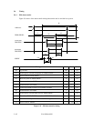
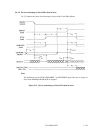
5.6.3.2 Ultra DMA data burst timing requirements
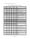
Table 5.16 Ultra DMA data burst timing requirements (1 of 2)
NAME MODE 0
(in ns)
MODE 1
(in ns)
MODE 2
(in ns)
COMMENT
MIN MAX MIN MAX MIN MAX
t
CYC
114 75 55 Cycle time (from STROBE edge to
STROBE edge)
t2
CYC
235 156 117 Two cycle time (from rising edge to next
rising edge or from falling edge to next
falling edge of STROBE)
t
DS
15 10 7 Data setup time (at recipient)
t
DH
5 5 5 Data hold time (at recipient)
t
DVS
70 48 34 Data valid setup time at sender (from data
bus being valid until STROBE edge)
t
DVH
6 6 6 Data valid hold time at sender (from
STROBE edge until data may become
invalid)
t
FS
0 230 0 200 0 170 First STROBE time (for device to first
negate DSTROBE from STOP during a
data in burst)
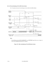
t
LI
0 150 0 150 0 150 Limited interlock time (see Note 1)
t
MLI
20 20 20 Interlock time with minimum (see Note 1)
t
UI
0 0 0 Unlimited interlock time (see Note 1)
t
AZ
10 10 10 Maximum time allowed for output drivers
to release (from being asserted or negated)
t
ZAH
20 20 20
t
ZAD
0 0 0
t
ENV
20 70 20 70 20 70 Envelope time (from DMACK- to STOP
and HDMARDY- during data in burst
initiation and from DMACK to STOP
during data out burst initiation)
t
SR
50 30 20 STROBE-to-DMARDY-time (if DMARDY-
is negated before this long after STROBE
edge, the recipient shall receive no more than
one additional data word)
t
RFS
75 60 50 Ready-to-final-STROBE time (no STROBE
edges shall be sent this long after negation
of DMARDY)
t
RP
160 125 100 Ready-to-pause time (that recipient shall
wait to initiate pause after negating
DMARDY-)
Minimum delay time required for output
drivers to assert or negate (from released
state)