


6
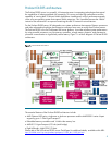
In the ProLiant DL585, processors access the memory controllers at core speed. Each on-chip memory
controller directly accesses the DIMMs on the same processor/memory board at the DIMM speed.
The aggregate bandwidth for locally accessed memory increases with the number of processors.
The Opteron chipset supports dual-channel memory, which reduces memory latency by increasing the
bus width from 64 bits + check bit to128 bits + check bits. Each memory controller is 64 bits wide
and is operated in lock-step to support the 128 bit interface. Because the ProLiant DL585 has dual-
width memory channels, DIMMs must be installed in pairs.
Overall memory speed and capacity for the DL585 is a function of the electrical loading and timing
constraints of the various types of memory. There are two different processor/memory boards used in
the ProLiant DL585 models. An 8-DIMM board supports PC2100 and PC2700 memory. A 4-DIMM
memory board supports PC3200 memory. The chart below breaks out the different configuration
options:
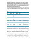
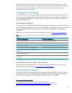
Table 2. Memory Configuration Options in the ProLiant DL585 server
Memory
type
Max
capacity
DIMM
size
Maximum
DIMMs per
processor
Memory
speed
Processor speeds
PC2100 64 GB 512 MB
1 GB
2 GB
8 266 MHz 1.6 – 2.4 GHz single-core
PC2700 128 GB 512 MB
1 GB
2 GB
4 GB
8
266 MHz > 2.4 GHz single-core, all dual-
core
PC2700 48 GB 512 MB
1 GB
2 GB
6 333 MHz > 2.4 GHz single-core, all dual-
core
PC2700 64 GB 4 GB 4 333 MHz > 2.4 GHz single-core, all dual-
core
PC3200 32 GB 512 MB
1 GB
2 GB
4 400 MHz > 2.6 GHz single-core, all dual-
core
To provide optimum performance for a wide variety of applications, the ProLiant DL585 can support
either of two methods of organizing memory access: linear, non-uniform memory access (NUMA), or
node interleaving sufficiently uniform memory accessing (SUMA).
A node consists of the processor, including the embedded memory controller and the attached DIMMs.
The total memory attached to all the processors is divided into 4096 byte segments. In the case of linear
addressing (NUMA), consecutive 4096 byte segments are on the same node. In the case of node
interleaving (SUMA), consecutive 4096 byte segments are on different or adjacent nodes.
• Linear memory accessing (NUMA) defines the memory starting at 0 on node 0 and assigns the total
amount of memory on node 0 the next sequential address, up to the memory total on node 0. The
memory on node 1 will then start with the next sequential address until the process is complete.
• Node interleaving (SUMA) breaks memory into 4-KB addressable entities. Addressing starts with
address 0 on node 0 and sequentially assigns through address 4095 to node 0, addresses 4096
through 8191 to node 1, addresses 8192 through 12287 to node 3, and addresses 12888