


4 RS/6000 7044 Model 170 Technical Overview
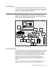
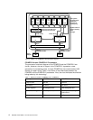
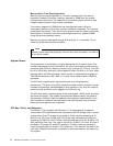
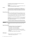
Figure 3. Model 170 - POWER3-II 400 MHz Block Diagram
POWER3 Versus POWER3-II Processors
The processor functional diagram of the POWER3 and the POWER3-II are
similar; however, the use of copper in the POWER3-II represents a new
generation of processing power. A single POWER3-II chip contains about 400
meters of copper wiring. Table 1 lists some of the differences between the
POWER3 and the POWER3-II processors. Also, the chart indicates the direction
being taken by this technology.
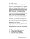
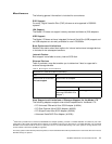
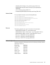
Table 1. Differences between POWER3 versus POWER3-II
Description POWER3 POWER3-II
Chip Die Size 270 mm
2
163 mm
2
Transistors 15 million 23 million
Power Avg/Max 39/46W@200 MHz 28W/36W@400 MHz
CMOS Technology 6S2, 5 layers metal 7S, 6 layers metal, copper
interconnect
Lithography 0.25
µm 0.22 µm
Floating
Point
Unit
FPU1
Floating
Point
Unit
FPU2
Fixed
Point
Unit
FXU1
Fixed
Point
Unit
FXU2
Fixed
Point
Unit
FXU3
LD/ST
Unit
LS1
LD/ST
Unit
LS2
Branch/Dispatch
Memory Mgmt Unit
Instruction Cache
IU
Memory Mgmt Unit
Data Cache
DU
BIU
Bus Interface Unit L2 Control, Clock
Branch history table 2048 entries
Branch target cache 256 entries
32 KB, 128-way 64 KB, 128-way
32
Bytes
32
Bytes
32 Bytes
@ 200 MHz=6.4 GB/s
16 Bytes
@ 100 MHz=1.6 GB/s
L2 Cache
4 MB
6XX Bus
CPU registers:
32 x 64-bit integer
(Fixed Point)
32 x 64-bit FP
(Floating Point)
Register buffers for
register renaming:
24 FP
16 Integer
Direct
Mapped