


112
CHAPTER 8 CLOCK OUTPUT CONTROL CIRCUIT
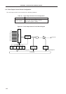
8.2 Clock Output Control Circuit Configuration
The clock output control circuit consists of the following hardware.
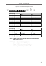
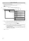
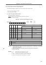
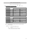
Table 8-1. Clock Output Control Circuit Configuration
Item Configuration
Timer clock select register 0 (TCL0)
Port mode register 3 (PM3)
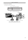
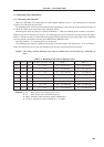
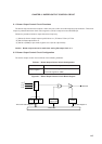
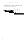
Figure 8-2. Clock Output Control Circuit Block Diagram
Control register
Internal Bus
f
XX
fXX/2
f
XX/2
2
fXX/2
3
fXX/2
4
fXX/2
5
fXX/2
6
fXX/2
7
CLOE TCL03 TCL02 TCL01 TCL00
P35
Output Latch
Synchronizing
Circuit
4
PM35
Selector
Timer Clock Select Register 0
Port Mode Register 3
PCL/P35