


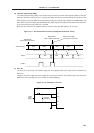

128
CHAPTER 10 A/D CONVERTER
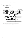
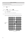
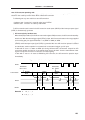
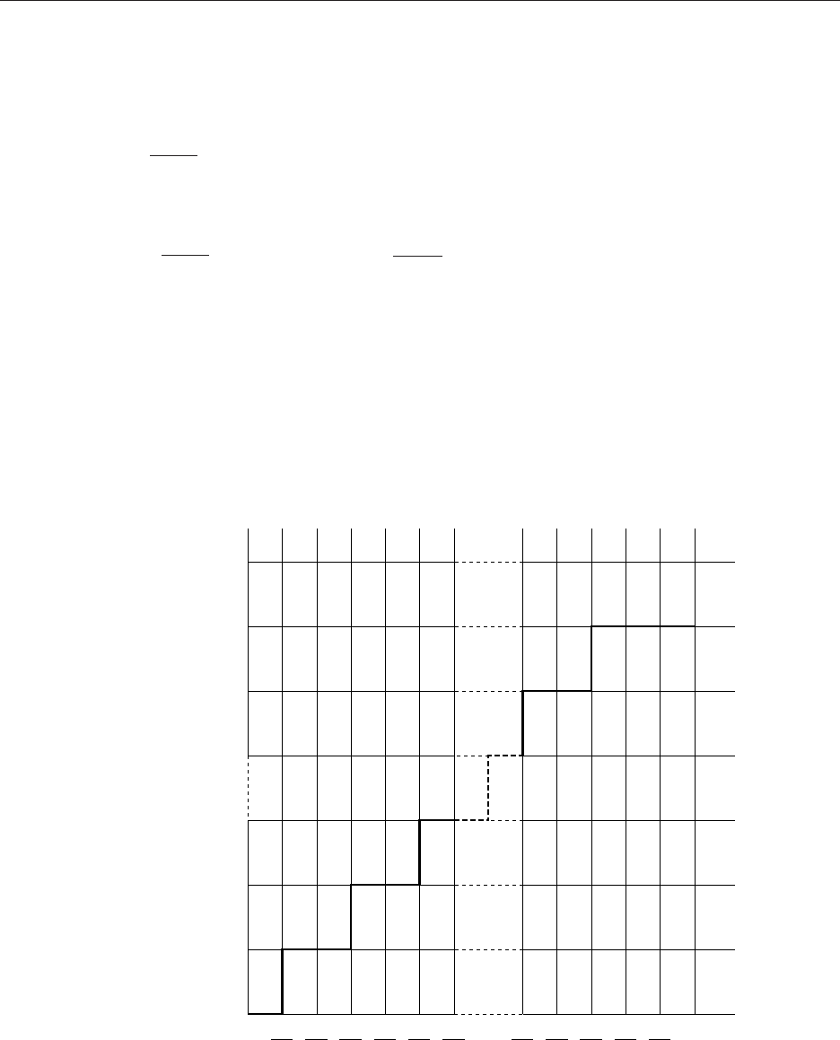
10.4.2 Input voltage and conversion results
The relation between the analog input voltage input to the analog input pins (ANI0 to ANI7) and the A/D conversion
result (the value stored in A/D conversion result register (ADCR)) is shown by the following expression.
ADCR = INT ( × 256 + 0.5)
or
(ADCR – 0.5) ×≤ V
IN < (ADCR + 0.5) ×
Where, INT( ) : Function which returns integer parts of value in parentheses.
V
IN : Analog input voltage
AV
REF : AVREF pin voltage
ADCR : Value of A/D conversion result register (ADCR)
Figure 10-6 shows the relation between the analog input voltage and the A/D conversion result.
Figure 10-6. Relations between Analog Input Voltage and A/D Conversion Result
VIN
AVREF
AVREF
256
AVREF
256
1
512
1
256
3
512
2
256
5
512
3
256
507
512
254
256
509
512
255
256
511
512
1
255
254
253
3
2
1
0
A/D Conversion
Results
(ADCR)
Input Voltage/AV
REF