


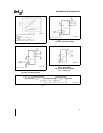
AUTOMOTIVE 80C51FA/83C51FA
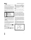
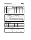
ABSOLUTE MAXIMUM RATINGS
Ambient Temperature
Under Bias...................................-40°C to +125°C
Storage Temperature.......................-65°C to +150°C
Voltage on Any Other Pin to V
SS........-0.5V to +6.5V
I
OL
I/O Pin........................................................15mA
Power Dissipation
(Based on PACKAGEheat transfer limitations, not
device power consumption)
Typical Junction Temperature (T
J
)................+135°C
(Based upon Ambient Temperature at
a
125
C)
Typical Thermal Resistance
Junction-to-Ambient (i
JA
)
PDIP.......................................................45°C/W
PLCC......................................................46°C/W
NOTICE: This is a production data sheet. The specifi-
cations are subject to change without notice.
WARNING: Stressing the device beyond the ``Absolute
Maximum Ratings'' may cause permanent damage.
These are stress ratings only. Operation beyond the
``Operating Conditions'' is not recommended and ex-
tended exposure beyond the ``Operating Conditions''
may affect device reliability.
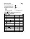
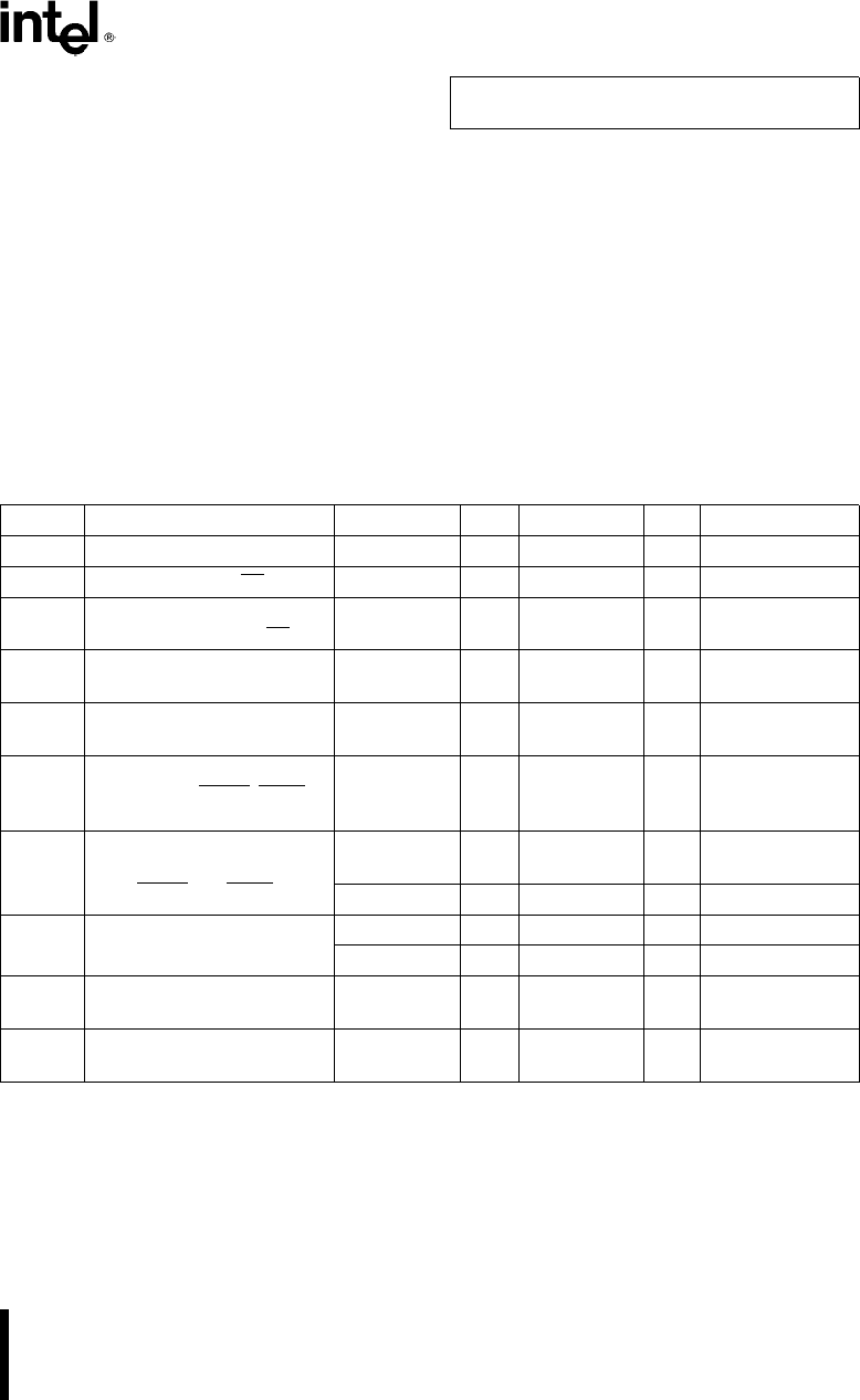
DC CHARACTERISTICS: (T
A
eb
40
Cto
a
125
C; V
CC
e
5V
g
10%; V
SS
e
0V)
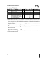
Symbol Parameter Min Typ Max Unit Test Conditions
V
IL
Input Low Voltage
b
0.5 0.2 V
CC
b
0.1 V
V
IL1
Input Low Voltage EA 0 0.2 V
CC
b
0.3 V
V
IH
Input High Voltage 0.2 V
CC
a
0.9 V
CC
a
0.5 V
(Except XTAL2, RST,EA
)
V
IH1
Input High Voltage 0.7V
CC
V
CC
a
0.5 V
(XTAL, RST)
V
OL
Output Low Voltage 0.45 V I
OL
e
1.6 mA
(1)
(Ports 1, 2 and 3)
V
OL1
Output Low Voltage 0.45 V I
OL
e
20
(Port 0, ALE/PROG
, PSEN)I
OL
e
3.2 mA
(1)
I
OL
e
7.0 mA
V
OH
Output High Voltage 2.4 V I
OH
eb
60 mA
(Ports 1, 2 and 3
ALE/PROG and PSEN)
0.9 V
CC
VI
OH
eb
10 mA
(2)
V
OH1
Output High Voltage 2.4 V I
OH
eb
800 mA
(Port 0 in External Bus Mode) 0.9 V
CC
VI
OH
eb
80 mA
(2)
I
IL
Logical 0 Input Current
b
10
b
50 mAV
IN
e
0.45V
(Ports 1, 2 and 3)
I
LI
Input leakage Current 0.02
g
10 mAV
IN
e
V
IL
or V
IH
(Port 0)
7