


Technical Reference
75
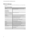
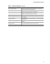
I/O Map
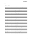
Table 31. I/O Map
Address (hex) Size Description
0000 - 000F 16 bytes DMA controller
0020 - 0021 2 bytes Programmable Interrupt Control (PIC)
0040 - 0043 4 bytes System timer
0060 1 byte Keyboard controller byte—reset IRQ
0061 1 byte System speaker
0064 1 byte Keyboard controller, CMD / STAT byte
0070 - 0071 2 bytes System CMOS / Real Time Clock
0072 - 0073 2 bytes System CMOS
0080 - 008F 16 bytes DMA controller
0092 1 byte Fast A20 and PIC
00A0 - 00A1 2 bytes PIC
00B2 - 00B3 2 bytes APM control
00C0 - 00DF 32 bytes DMA
00F0 1 byte Numeric data processor
0170 - 0177 8 bytes Secondary IDE channel
01F0 - 01F7 8 bytes Primary IDE channel
0228 - 022F* 8 bytes LPT3
0278 - 027F* 8 bytes LPT2
02E8 - 02EF* 8 bytes COM4 / video (8514A)
02F8 - 02FF* 8 bytes COM2
0376 1 byte Secondary IDE channel command port
0377, bits 6:0 7 bits Secondary IDE channel status port
0378 - 037F 8 bytes LPT1
03B0 - 03BB 12 bytes Video (VGA)
03C0 - 03DF 32 bytes Video (VGA)
03E8 - 03EF 8 bytes COM3
03F0 - 03F5 6 bytes Diskette channel 1
03F6 1 byte Primary IDE channel command port
03F8 - 03FF 8 bytes COM1
04D0 - 04D1 2 bytes Edge / level triggered PIC
LPTn + 400 8 bytes ECP port, LPTn base address + 400h
0CF8 - 0CFB** 4 bytes PCI configuration address register
0CF9*** 1 byte Turbo and reset control register
0CFC - 0CFF 4 bytes PCI configuration data register
FFA0 - FFA7 8 bytes Primary bus master IDE registers
FFA8 - FFAF 8 bytes Secondary bus master IDE registers
continued