LXD381 — Evaluation Board for Octal E1 Applications
8 Developer Manual
2.5 Receive Polarity Selection
The polarity of RPOS/RNEG is determined by the CLKE switch in switch block S2. When the
CLKE switch is OFF, RPOS/RNEG are active Low. When set to the ON position, RPOS/RNEG
are active High. Note that the CLKE switch controls the LXT381’s RPOL pin.
2.6 Output Enable Selection
The OE switch in switch block S3 controls the operation of the LXT381 output drivers. For normal
operation (driver outputs enabled), set the OE switch to the ON position. Setting the OE switch to
OFF forces the output drivers to the high impedance state.
2.7 Unused Switches
Switches 3 and 4, in switch block S2, have no function on the LXD381 and should be set to the
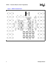
OFF position. Figure 2 shows the factory default settings for switch block S2.
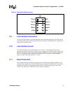
2.8 Back-End Interface Connection
Eight 10 pin connectors (JP1 - JP8) provide access to the LXT381 digital signals to allow
interfacing the back-end Framer/Mapper or ASIC with an external pattern generator. Figure 3
shows a typical connector (JP1 for channel 0) with the factory installed jumper connecting RCLK
to TCLK. This jumper is normally installed when feeding analog test data from the line interface
(TIP and RING).
Figure 2. S2 Factory Switch Settings
1 2 3 4
O
F
F
CLKE
OE
S2
NOTE: OFF position = Low


